|
|
|
PDF AD8231 Data sheet ( Hoja de datos )
| Número de pieza | AD8231 | |
| Descripción | Digital Programmable Instrumentation Amplifier | |
| Fabricantes | Analog Devices | |
| Logotipo | ||
Hay una vista previa y un enlace de descarga de AD8231 (archivo pdf) en la parte inferior de esta página. Total 25 Páginas | ||
|
No Preview Available !
Data Sheet
Zero Drift, Digitally Programmable
Instrumentation Amplifier
AD8231
FEATURES
Digitally/pin-programmable gain
G = 1, 2, 4, 8, 16, 32, 64, or 128
Specified from −40°C to +125°C
50 nV/°C maximum input offset drift
10 ppm/°C maximum gain drift
Excellent dc performance
80 dB minimum CMR, G = 1
15 μV maximum input offset voltage
500 pA maximum bias current
0.7 μV p-p noise (0.1 Hz to 10 Hz)
Good ac performance
2.7 MHz bandwidth, G = 1
1.1 V/μs slew rate
Rail-to-rail output
Shutdown/multiplex
Extra op amp
Single-supply range: 3 V to 5 V
Dual-supply range: ±1.5 V to ±2.5 V
Qualified for automotive applications
APPLICATIONS
Pressure and strain transducers
Thermocouples and RTDs
Programmable instrumentation
Industrial controls
Weigh scales
Automotive controls
GENERAL DESCRIPTION
The AD8231 is a low drift, rail-to-rail, instrumentation amplifier
with software-programmable gains of 1, 2, 4, 8, 16, 32, 64, or 128.
The gains are programmed via digital logic or pin strapping.
The AD8231 is ideal for applications that require precision
performance over a wide temperature range, such as industrial
temperature sensing and data logging. Because the gain setting
resistors are internal, maximum gain drift is only 10 ppm/°C for
gains of 1 to 32. Because of the auto-zero input stage, maximum
input offset is 15 μV and maximum input offset drift is just
50 nV/°C. CMRR is 80 dB for G = 1, increasing to 110 dB at
higher gains.
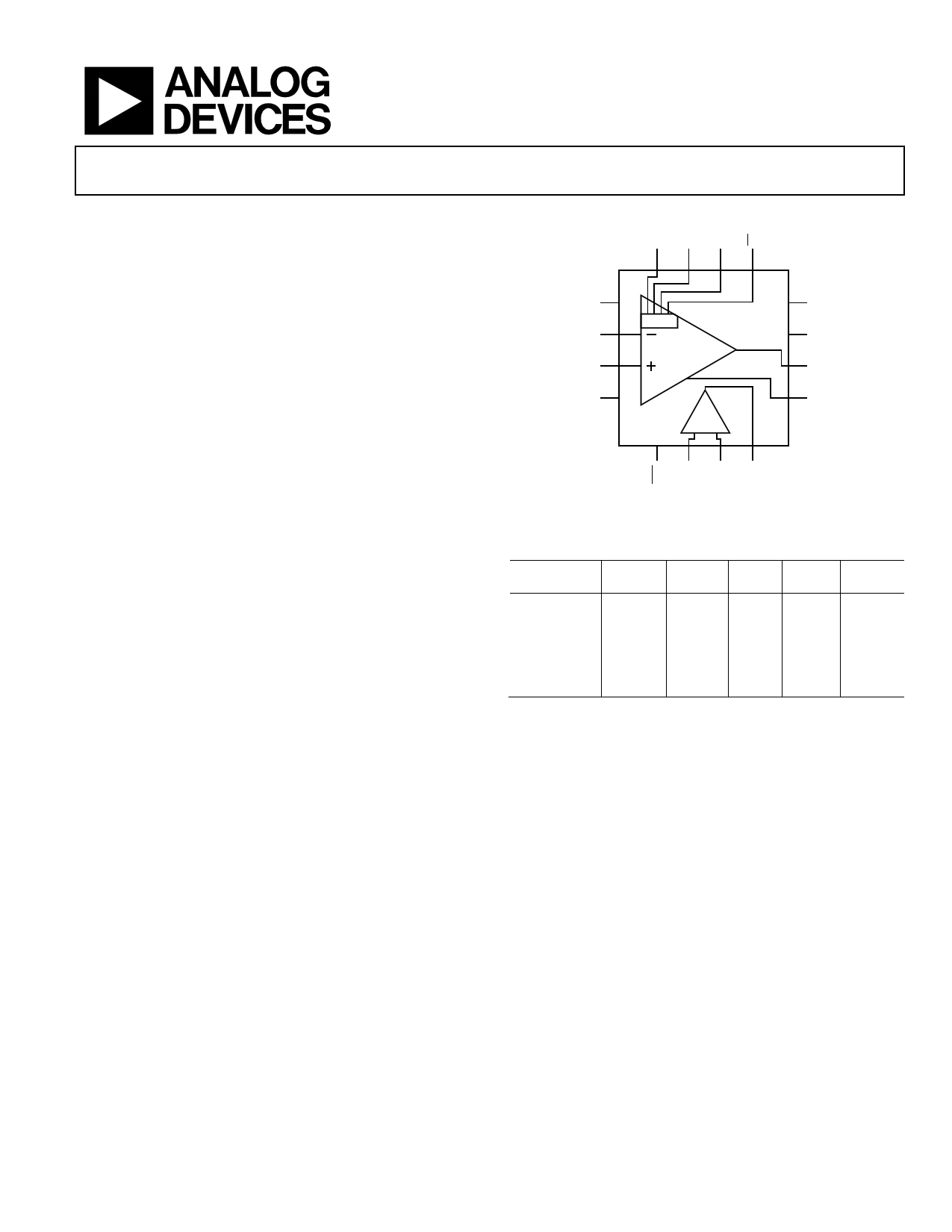
FUNCTIONAL BLOCK DIAGRAM
1
NC
–INA 2
+INA 3
LOGIC
IN-AMP
NC 4
AD8231
OP
AMP
12
+VS
11
–VS
10 OUTA
9 REF
Figure 1.
Table 1. Instrumentation and Difference Amplifiers by
Category
High
Low
Performance Cost
High Mil Low Digital
Voltage Grade Power Gain
AD8221
AD6231 AD628 AD620 AD6271 AD82311
AD82201
AD85531 AD629 AD621
AD8250
AD8222
AD524
AD8251
AD82241
AD526
AD85551
AD624
AD85561
AD85571
1 Rail-to-rail output.
The AD8231 also includes an uncommitted op amp that can be
used for additional gain, differential signal driving, or filtering.
Like the in-amp, the op amp has an auto-zero architecture, rail-
to-rail input, and rail-to-rail output.
The AD8231 includes a shutdown feature that reduces current
to a maximum of 1 μA. In shutdown, both amplifiers also have
a high output impedance, which allows easy multiplexing of
multiple amplifiers without additional switches.
The AD8231 is specified over the extended industrial tempera-
ture range of −40°C to +125°C. It is available in a 4 mm × 4 mm
16-lead LFCSP.
Rev. C
Document Feedback
Information furnished by Analog Devices is believed to be accurate and reliable. However, no
responsibility is assumed by Analog Devices for its use, nor for any infringements of patents or other
rights of third parties that may result from its use. Specifications subject to change without notice. No
license is granted by implication or otherwise under any patent or patent rights of Analog Devices.
Trademarksandregisteredtrademarksarethepropertyoftheirrespectiveowners.
One Technology Way, P.O. Box 9106, Norwood, MA 02062-9106, U.S.A.
Tel: 781.329.4700 ©2007–2014 Analog Devices, Inc. All rights reserved.
Technical Support
www.analog.com
1 page 
AD8231
Parameter
Dynamic Performance
Bandwidth
G=1
G=2
Gain Bandwidth Product
G = 4 to 128
Slew Rate
Output Characteristics
Output Voltage High
Output Voltage Low
Short-Circuit Current
Digital Interface
Input Voltage Low
Input Voltage High
Setup Time to CS High
Hold Time after CS High
OPERATIONAL AMPLIFIER
Input Characteristics
Offset Voltage, VOS
Temperature Drift
Input Bias Current
Input Offset Current
Input Voltage Range
Open-Loop Gain
Common-Mode Rejection Ratio
Power Supply Rejection Ratio
Voltage Noise Density
Voltage Noise
Dynamic Performance
Gain Bandwidth Product
Slew Rate
Output Characteristics
Output Voltage High
Output Voltage Low
Short-Circuit Current
BOTH AMPLIFIERS
Power Supply
Quiescent Current
Quiescent Current (Shutdown)
Conditions
RL = 100 kΩ to ground
RL = 10 kΩ to ground
RL = 100 kΩ to 5 V
RL = 10 kΩ to 5 V
TA = −40°C to +125°C
TA = −40°C to +125°C
TA = −40°C to +125°C
TA = −40°C to +125°C
TA = −40°C to +125°C
TA = −40°C to +125°C
TA = −40°C to +125°C
f = 0.1 Hz to 10 Hz
RL = 100 kΩ to ground
RL = 10 kΩ to ground
RL = 100 kΩ to 5 V
RL = 10 kΩ to 5 V
Data Sheet
Min Typ Max Unit
2.7 MHz
2.5 MHz
7 MHz
1.1 V/µs
4.9 4.94
V
4.8 4.88
V
60 100 mV
80 200 mV
70 mA
1.0 V
4.0 V
50 ns
20 ns
5
0.01
250
20
0.05
100 120
100 120
100 110
20
0.4
1
0.5
4.9 4.96
4.8 4.92
60
80
70
15 µV
0.06 µV/°C
500 pA
5 nA
100 pA
0.5 nA
4.95 V
V/mV
dB
dB
nV/√Hz
µV p-p
MHz
V/µs
V
V
100 mV
200 mV
mA
45
0.01 1
mA
µA
Rev. C | Page 4 of 24
5 Page 
AD8231
2000
VREF = MIDSUPPLY
VCM = MIDSUPPLY
1500
1000
500
3V
0
5V
–500
–40 –20
0
20 40 60 80
TEMPERATURE (°C)
100 120
Figure 9. Instrumentation Amplifier Bias Current vs. Temperature
2.0
1.5
1.0
0.5
0
–0.5
–1.0
–1.5
–2.0
–2.5 –2.0 –1.5 –1.0 –0.5 0
+VS = +2.5V
–VS = –2.5V
VREF = 0V
0.5 1.0 1.5 2.0 2.5
VCM (V)
Figure 10. Instrumentation Amplifier Bias Current vs.
Common-Mode Voltage, 5 V
1.0
0.8
0.6
0.4
0.2
0
–0.2
–0.4
–0.6
–0.8
–1.0
–1.5 –1.2 –0.9 –0.6 –0.3 0
+VS = +1.5V
–VS = –1.5V
VREF = 0V
0.3 0.6 0.9 1.2 1.5
VCM (V)
Figure 11. Instrumentation Amplifier Bias Current vs.
Common-Mode Voltage, 3 V
Data Sheet
6
0V, 4.96V
5
4
5V SINGLE SUPPLY
3
4.92V, 2.5V
2 0V, 2.96V
3V SINGLE SUPPLY
1
0V, 0.04V
2.92V, 1.5V
0
0123456
OUTPUT VOLTAGE (V)
Figure 12. Instrumentation Amplifier Input Common-Mode Range vs.
Output Voltage, All Gains, VREF = 0 V
6
1.5V, 4.96V
5
4 0.02V, 4.22V 5V SINGLE SUPPLY
1.5V, 2.96V
3
4.98V, 3.22V
2 0.02V, 2.22V
2.98V, 2.22V
3V SINGLE SUPPLY
4.98V, 1.78V
1 0.02V, 0.78V
2.98V, 0.78V
1.5V, 0.04V
0
0 0.5 1.0 1.5 2.0 2.5 3.0 3.5 4.0 4.5 5.0
OUTPUT VOLTAGE (V)
Figure 13. Instrumentation Amplifier Input Common-Mode Range vs.
Output Voltage, All Gains, VREF = 1.5 V
6
2.5V, 4.96V
5
4
0.02V, 3.72V
5V SINGLE SUPPLY
4.98V, 3.72V
3
2.5V, 2.96V 2.98V, 2.72V
2
0.02V, 1.72V
1
3V SINGLE
SUPPLY
4.98V,1.28V
0.02V, 1.28V
2.5V, 0.04V
2.98V, 0.28V
0
0 0.5 1.0 1.5 2.0 2.5 3.0 3.5 4.0 4.5 5.0
OUTPUT VOLTAGE (V)
Figure 14. Instrumentation Amplifier Input Common-Mode Range vs.
Output Voltage, All Gains, VREF = 2.5 V
Rev. C | Page 10 of 24
11 Page | ||
| Páginas | Total 25 Páginas | |
| PDF Descargar | [ Datasheet AD8231.PDF ] | |
Hoja de datos destacado
| Número de pieza | Descripción | Fabricantes |
| AD823 | Dual/ 16 MHz/ Rail-to-Rail FET Input Amplifier | Analog Devices |
| AD8230 | Precision Instrumentation Amplifier | Analog Devices |
| AD8231 | Digital Programmable Instrumentation Amplifier | Analog Devices |
| AD8232 | Heart Rate Monitor Front End | Analog Devices |
| Número de pieza | Descripción | Fabricantes |
| SLA6805M | High Voltage 3 phase Motor Driver IC. |
Sanken |
| SDC1742 | 12- and 14-Bit Hybrid Synchro / Resolver-to-Digital Converters. |
Analog Devices |
|
DataSheet.es es una pagina web que funciona como un repositorio de manuales o hoja de datos de muchos de los productos más populares, |
| DataSheet.es | 2020 | Privacy Policy | Contacto | Buscar |