|
|
|
PDF AD1996 Data sheet ( Hoja de datos )
| Número de pieza | AD1996 | |
| Descripción | Class-D Audio Power Amplifier | |
| Fabricantes | Analog Devices | |
| Logotipo | ||
Hay una vista previa y un enlace de descarga de AD1996 (archivo pdf) en la parte inferior de esta página. Total 16 Páginas | ||
|
No Preview Available !
Preliminary Technical Data
FEATURES
Integrated Stereo Modulator & Power Stage
0.005% THD+N
101.5dB Dynamic Range
PSRR > 65 dB
RDS-ON < 0.3 Ω (per transistor)
Efficiency > 80% @ 5W/6 Ω
EMI Optimized Modulator
On-Off-Mute Pop Noise Suppression
Short Circuit Protection
Over-Temperature Protection
Low Cost DMOS Process
APPLICATIONS
Flat Panel Televisions
Automotive Amplifiers
PC Audio Systems
Mini Components
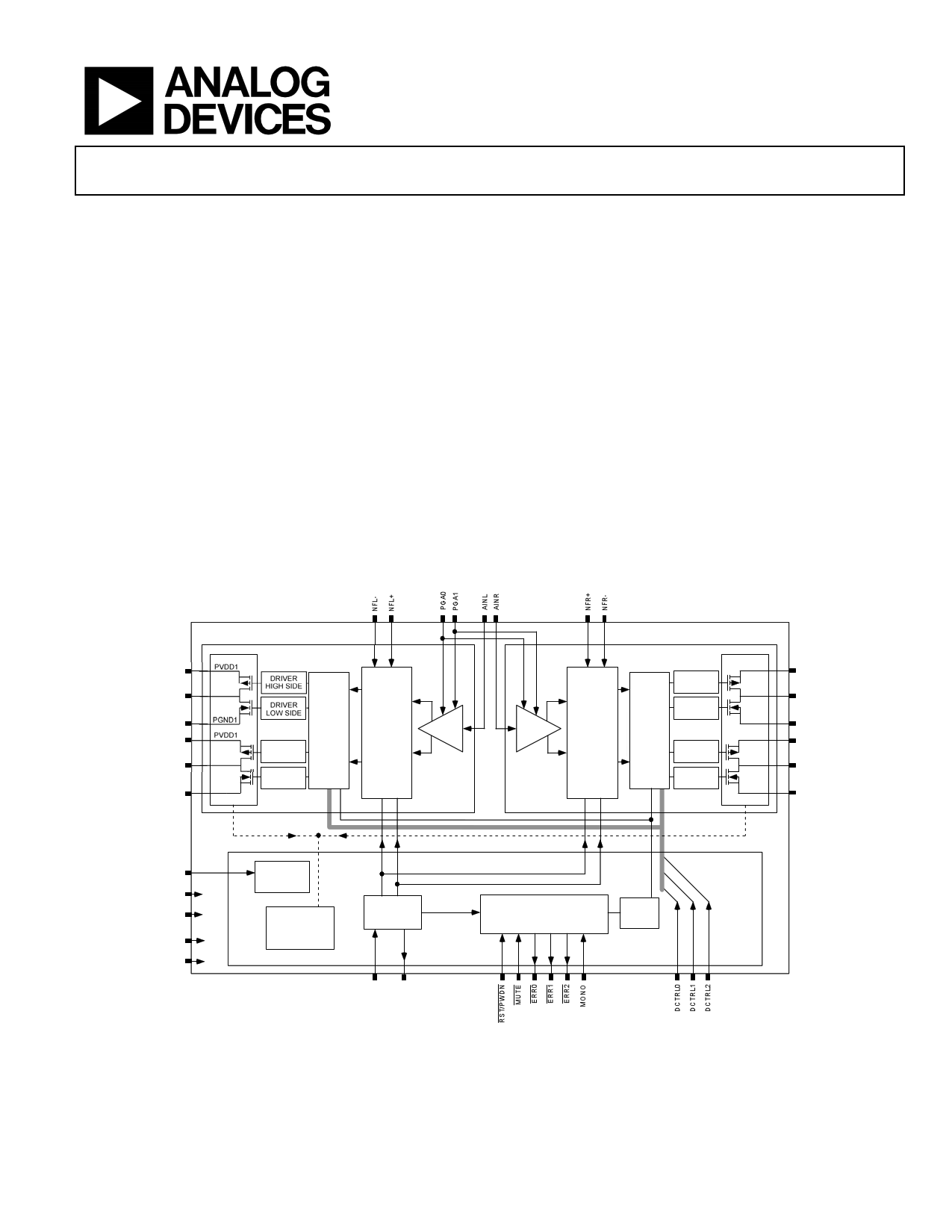
Class-D Audio Power Amplifier
AD1990/AD1992/AD1994/AD1996
GENERAL DESCRIPTION
The AD199x is a two channel Bridge Tied Load (BTL)
switching audio power amplifier with integrated ∑∆ modulator.
The modulator accepts a 1Vrms input signal (maximum power)
and generates a switching waveform to drive speakers directly.
One of the two modulators can control both output stages
providing twice the current for single-channel applications. A
digital, microcontroller-compatible interface provides control of
reset, mute and PGA gain as well as output signals for thermal
and over-current error conditions. The output stage can operate
from supply voltages ranging from 8V to 20V. The analog
modulator and digital logic operate from a 5V supply.
AD1990: 5Wx2 (10Wx1)
AD1992: 10Wx2 (20Wx1)
AD1994: 25Wx2 (50Wx1)
AD1996: 40Wx2 (80Wx1)
62 63
3w2 ww.D3a1taS6h0eet4U5.c3om
7,8
PVDD
4,5,6
OUTL+
1,2,3
PGND1
9,10
PVDD1
11,12,13
OUTL-
14,15,16
PGND1
PGND1
LEFT CHANNEL
DRIVER
HIGH SIDE
LEVEL
SHIFT
+
DEAD
TIME
CONTROL
DRIVER
LOW SIDE
Σ∆
M O D U L AT O R
PGA
PGA
50 51
RIGHT CHANNEL
Σ∆
M O D U L AT O R
DRIVER
HIGH SIDE
LEVEL
SHIFT
+
DEAD
TIME
CONTROL
DRIVER
LOW SIDE
DRIVER
HIGH SIDE
DRIVER
LOW SIDE
PVDD2
PGND2
PVDD2
PGND2
41,42
PVDD2
43,44,45
OUTR+
46,47,48
PGND2
39,40
PVDD2
36,37,38
OUTR-
33,34,35
PGND2
55
R E F _ F ILT
57
AV D D
56
AGND
24,25
DVDD
23,26
DGND
V O LTA G E
REFERENCE
T E M P E R AT U R E
SENSE &
OVER-CURRENT
PROTECTION
Ø1 Ø2
O S C ILL ATO R
27 28
CLKI CLKO
Ø1 Ø2
MODE CONTROL LOGIC
MUTE/
POP
CONTROL
30 29 19 18 17 49
22 21 20
Figure 1. Block Diagram
Rev. PrA – 1/20/05
Information furnished by Analog Devices is believed to be accurate and reliable.
However, no responsibility is assumed by Analog Devices for its use, nor for any
infringements of patents or other rights of third parties that may result from its use.
Specifications subject to change without notice. No license is granted by implication
or otherwise under any patent or patent rights of Analog Devices. Trademarks and
registered trademarks are the property of their respective companies.
One Technology Way, P.O. Box 9106, Norwood, MA 02062-9106, U.S.A.
Tel: 781.329.4700
www.analog.com
Fax: 781.326.8703 © 2005 Analog Devices, Inc. All rights reserved.
1 page 
Preliminary Technical Data
AD199x
Table 2 DIGITAL TIMING (Guaranteed over -40°C to +85°C, AVDD = DVDD = 5.0V ± 10%, PVDDX =12V ± 10%, Non Overlap Time
tNOL = Shortest, See Table 6: Non-Overlap Time Settings)
Parameter
Min Typ Max
Units
Comments
tPDRP
500
ns RST/PDN minimum low pulsewidth
tMPDL 5 µs MUTE asserted to output initial response
tMUTEDLY
1 sec RST/PDN high to MUTE high delay
OUTL+/
OUTR+
OUTL-/
OUTR-
tNOL
tNOL
Figure 2. Output Timing
MUTE
OUTX
tPST
tPST
tMPDL
Figure 3. Mute Timing
tMPDL
RESET
MUTE
tMUTEDLY
Figure 4. Reset to Mute Delay
Rev. PrA – 1/20/05 | Page 5 of 16
5 Page 
Preliminary Technical Data
Programmable Gain Amplifier (PGA)
The AD199x incorporates a single-ended to differential
converter for each channel in the analog front-end section. Both
single-ended to differential converters feature a programmable
gain amplifier with four different gain settings. The gain is set
using the pins PGA1 and PGA0 as shown in Table 5. The
PGA1 and PGA0 pins are continuously monitored allow the
gain to be changed at any time.
Table 5. PGA Gain Settings
PGA1
PGA0
00
01
10
11
PGA Gain (dB)
0
6
12
18
SYSTEM DESIGN
Clocking
The AD199x has two clock pins, CLKI and CLKO which are
used to configure the clocking scheme for the device. The
AD199x should be driven by a clock which is 256 × fS where fS
is the desired sampling rate. If a crystal is to be used as the
clock source it should be connected across the CLKI and
CLKO pins as shown in Figure 17. Crystal Connection The
values and type of capacitors used will be determined by the
crystal manufacturer. A square-wave clock source may be
connected directly to the CLKI pin. The logic levels of the
square wave should be compatible with those defined in the
Digital I/O section of the specifications page.
22pF
XTAL
47Ω
22pF
Figure 17. Crystal Connection
Output Transistor Non-Overlap Time
Ipsum lorum...
Power-up Considerations
Careful power-up is necessary when using the AD199x to
ensure correct operation and avoid possible latch-up issues. The
AD199x should be powered-up with RST/PDN and MUTE
held low until all the power supplies have stabilized. Once the
supplies have stabilized the AD199x can be brought out of reset
by bringing RST/PDN high and then MUTE can be brought
AD199x
high as required.
On/Off/Mute Pop Noise Suppression
The AD199x features pop suppression which is activated when
the part is reset or taken out of mute. The pop suppression is
achieved by pulsing the power outputs to bring the outputs of
the LC filter from 0V to mid-scale in a controlled fashion. This
feature eliminates unwanted transients on both the outputs and
the high voltage power supply.
Thermal Protection
The AD199x features thermal protection. When the die
temperature exceeds approximately 135°C the Thermal
Warning Error output (ERR1) is asserted. If the die temperature
exceeds approximately 150°C the Thermal Shutdown Error
output (ERR2) is asserted. If this occurs, the part shuts down to
prevent damage to the part. When the die temperature drops
below approximately 120°C both error outputs are negated and
the part returns to normal operation.
Over-current Protection
The AD199x features over current or short circuit protection. If
the current through any power transistors exceeds 4A the part
goes into mute and the Over-current error output (ERR0) is
asserted. This is a latched error and does not clear
automatically. To clear the error condition and restore normal
operation, the part must be either reset, or MUTE must be
asserted and negated.
Application Considerations
Good board layout and decoupling are vital for correct
operation of the AD199x. Due to the fact that the part switches
high currents there is the potential for large PVDD bounce each
time a transistor transitions. This can cause unpredictable
operation of the part. To avoid this potential problem, close
chip decoupling is essential. It is also recommended that the
decoupling capacitors are placed on the same side of the board
as the AD199x, and connected directly to the PVDD and
PGND pins. By placing the decoupling capacitors on the other
side of the board and decoupling through vias the effectiveness
of the decoupling is reduced. This is because vias have
inductive properties and therefore prevent very fast discharge
of the decoupling capacitors. Best operation is achieved with at
least one decoupling capacitor on each side of the AD199x, or
optionally two capacitors per side can be used to further reduce
the series resistance of the capacitor. If these decoupling
recommendations cannot be followed and decoupling through
vias is the only option, the vias should be made as large as
possible to increase surface area, thereby reducing inductance
and resistance.
Rev. PrA – 1/20/05 | Page 11 of 16
11 Page | ||
| Páginas | Total 16 Páginas | |
| PDF Descargar | [ Datasheet AD1996.PDF ] | |
Hoja de datos destacado
| Número de pieza | Descripción | Fabricantes |
| AD1990 | Audio Switching Amplifier | Analog Devices |
| AD1991 | Class D/1-Bit Audio Power Output Stage | Analog Devices |
| AD1992 | Audio Switching Amplifier | Analog Devices |
| AD1994 | Audio Switching Amplifier | Analog Devices |
| Número de pieza | Descripción | Fabricantes |
| SLA6805M | High Voltage 3 phase Motor Driver IC. |
Sanken |
| SDC1742 | 12- and 14-Bit Hybrid Synchro / Resolver-to-Digital Converters. |
Analog Devices |
|
DataSheet.es es una pagina web que funciona como un repositorio de manuales o hoja de datos de muchos de los productos más populares, |
| DataSheet.es | 2020 | Privacy Policy | Contacto | Buscar |