|
|
|
PDF NCN2500 Data sheet ( Hoja de datos )
| Número de pieza | NCN2500 | |
| Descripción | USB Single Channel Transceiver | |
| Fabricantes | ON Semiconductor | |
| Logotipo | ||
Hay una vista previa y un enlace de descarga de NCN2500 (archivo pdf) en la parte inferior de esta página. Total 14 Páginas | ||
|
No Preview Available !
NCN2500
USB Single Channel
Transceiver
The NCN2500 Integrated Circuit is a single channel transceiver
designed to accommodate the physical USB Port with a
microcontroller digital I/O. The part is fully USB compliant and
supports the full 12 Mbps speed. On the other hand, the NCN2500
device includes the pullup resistors as defined by the USB−ECN new
specifications.
Features
• Compliant to the USB Specification, Version 2.0, Low and Full
Speed
• Very Small Footprint Due to the QFN−16 Package
• Integrated D+/D− Pullup Resistors
• Operates Over the Full 1.5 V to 3.6 V Supply
• Pb−Free Package is Available*
Typical Applications
• Portable Computer
• Cellular Phone
http://onsemi.com
MARKING
DIAGRAM
16
1
QFN−16
MNR SUFFIX
1 CASE 485G
XXXX
ALYW
G
A = Assembly Location
L = Wafer Lot
Y = Year
W = Work Week
G = Pb−Free Package
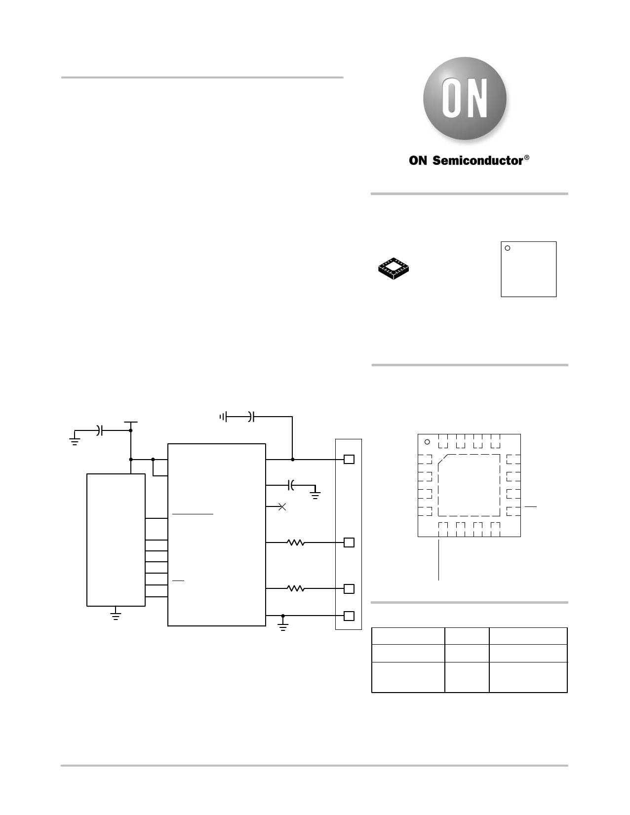
C1 Vcc
GND
10 mF
GND
15 Vcc
16 EN_RPU
mC
GND
5 EN_VObus
2 RCV
3 Vp
4 Vm
1 DSPD
9 OE
7 SPND
NCN2500
C2
4.7 mF
www.DataSheet4U.com
Vusb 14
Vreg 12 C3
VObus 13
1 mF
GND
1
D− 10 R2
33 R
2
D+ 11
GND 6
R3
33 R
GND
3
4
Figure 1. Typical Application
*For additional information on our Pb−Free strategy and soldering details, please
download the ON Semiconductor Soldering and Mounting Techniques
Reference Manual, SOLDERRM/D.
PIN CONNECTIONS
DSPD 1
RCV 2
Vp 3
Vm 4
16 15 14 13
12 Vreg
11 D+
10 D−
9 OE
5 6 78
(Top View)
ORDERING INFORMATION
Device
Package
Shipping†
NCN2500MNR2 QFN−16 3000 Tape & Reel
NCN2500MNR2G QFN−16 3000 Tape & Reel
(Pb−Free)
†For information on tape and reel specifications,
including part orientation and tape sizes, please
refer to our Tape and Reel Packaging Specifications
Brochure, BRD8011/D.
© Semiconductor Components Industries, LLC, 2005
November, 2005 − Rev. 2
1
Publication Order Number:
NCN2500/D
1 page 
NCN2500
ELECTRICAL CHARACTERISTICS
Characteristic
Symbol
Pin
Min Typ Max
DIGITAL PARAMETERS SECTION @ 1.5 V < Vcc < 3.6 V (−40°C to +85°C ambient temperature, unless otherwise noted.)
NOTE: Digital inputs undershoot < −0.3 V to ground, digital inputs overshoot < 0.3 V to Vcc.
High Level Input Voltage DSPD, Vp, Vm, EN_VObus,
SPND, OE, EN_RPU
VIH 1, 3, 4, 5, 0.80*Vcc
7, 9, 16
−
−
Low Level Input Voltage DSPD, Vp, Vm, EN_VObus,
SPND, OE, EN_RPU
VIL 1, 3, 4, 5,
7, 9, 16
−
− 0.20*Vcc
High Level Output Voltage RCV, Vp, Vm @ IOH = 1.0 mA
VOH
2, 3, 4
0.80*Vcc
Low Level Output Voltage RCV, Vp, Vm @ IOL = 1.0 mA VOL 2, 3, 4
−
Input Leakage Current DSPD, Vp, Vm, EN_VObus,
SPND, OE, EN_RPU
IIL 1, 3, 4, 5,
7, 9, 16
−
−−
− 0.20*Vcc
− "5.0
Input EN_RPU Pulldown Resistor @VCC = 3.3 V
RPU
−
− 300 −
TRANSCEIVER SECTION @ 1.5 V < Vcc < 3.6 V (−40°C to +85°C ambient temperature, unless otherwise noted.)
Static Output High, D−, D+ @ OE = Low, RL = 15 kΩ
to GND
VOH
10, 11
2.8
−
3.6
Static Output Low, D−, D+ @ OE = Low, RL = 1.5 kΩ
to Vreg
VOL 10, 11
−
− 0.3
Single Input Receiver Threshold
Single Ended Receiver Hysteresis (Note 3)
VSE 10, 11
−−
0.8
−
− 2.0
200 −
Differential Input Sensitivity | D+ − D− | @ 0.8 V < VCM
VDI 10, 11
0.2
−
−
< 2.5 V (Note 3)
Differential Common Mode Including the VDI
Differential Receiver Hysteresis (Note 3)
VCM
−
10, 11
10, 11
0.8
−
− 2.5
70 −
D+ and D− Transceiver Hi−Z State Leakage Current @
OE = 1, 0 V < Vusb < 3.3 V
ILO 10, 11
−
− "10
Transceiver Input Capacitance (Note 3)
Cin 10, 11
−
− 20
Transceiver Output Resistance (Note 3)
Transceiver Input Impedance (Note 3)
Internal RPU1 Pull Resistor
Internal RPU2 Pull Up Resistor
ZDRV
ZIN
RRPU−1
RRPU−2
10, 11
10, 11
10, 12
10, 12
28
10
900
525
− 44
−−
− 1575
− 1515
LOW SPEED DRIVER OPERATION (Note 3)
Transition Rise Time
@ CL = 50 pF
@ CL = 600 pF
Transition Fall Time
@ CL = 50 pF
@ CL = 600 pF
Rise and Fall Time Matching
tr 10, 11
tf 10, 11
tr, tf 10, 11
75
75
75
75
80
− 300
− 300
− 300
− 300
− 125
Output Signal Crossover Voltage
Data Transaction Rate
3. Parameter guaranteed by design, not production tested.
VCRS
Drate
10, 11
10, 11
1.3
−
− 2.0
− 1.5
Unit
V
V
V
V
mA
kW
V
V
V
mV
V
V
mV
mA
pF
W
MW
W
W
ns
ns
%
V
Mbs
http://onsemi.com
5
5 Page 
NCN2500
TYPICAL APPLICATIONS
GND
Vcc
C1
4.7 mF
mC
GND
GND
U1
C2
4.7 mF
15 Vcc
16 EN_RPU
5 EN_VObus
Vusb 14
Vreg 12
VObus 13
C3
1 mF
2 RCV
3 Vp
4 Vm
1 DSPD
9 OE
7 SPND
D− 10
D+ 11
GND 6
R2
33 R
R3
33 R
NCN2500
GND
GND
1
2
3
4
In this application, the two internal pullup resistors (RPU1 and RPU2) are used to bias the USB line.
Consequently, the VObus voltage is deactivated (Pin 5 connected to Vcc).
Figure 10. Fully Independent Power Supplies
C2
4.7 mF
RS232
PORT
GND
GND
mC
GND
U1
15 Vcc
16 EN_RPU
5 EN_VObus
2 RCV
3 Vp
4 Vm
1 DSPD
9 OE
7 SPND
NCN2500
Vusb 14
Vreg 12
VObus 13
C3
GND
1 mF
D− 10
D+ 11
GND 6
GND
R2
33 R
R3
33 R
Figure 11. Peripheral are Powered by the Vreg Supply
1
2
3
4
http://onsemi.com
11
11 Page | ||
| Páginas | Total 14 Páginas | |
| PDF Descargar | [ Datasheet NCN2500.PDF ] | |
Hoja de datos destacado
| Número de pieza | Descripción | Fabricantes |
| NCN2500 | USB Single Channel Transceiver | ON Semiconductor |
| Número de pieza | Descripción | Fabricantes |
| SLA6805M | High Voltage 3 phase Motor Driver IC. |
Sanken |
| SDC1742 | 12- and 14-Bit Hybrid Synchro / Resolver-to-Digital Converters. |
Analog Devices |
|
DataSheet.es es una pagina web que funciona como un repositorio de manuales o hoja de datos de muchos de los productos más populares, |
| DataSheet.es | 2020 | Privacy Policy | Contacto | Buscar |