|
|
|
PDF NTMS5P02R2 Data sheet ( Hoja de datos )
| Número de pieza | NTMS5P02R2 | |
| Descripción | Power MOSFET ( Transistor ) | |
| Fabricantes | ON Semiconductor | |
| Logotipo | ||
Hay una vista previa y un enlace de descarga de NTMS5P02R2 (archivo pdf) en la parte inferior de esta página. Total 7 Páginas | ||
|
No Preview Available !
NTMS5P02R2
Power MOSFET
−5.4 Amps, −20 Volts
P−Channel Enhancement−Mode
Single SOIC−8 Package
Features
• High Density Power MOSFET with Ultra Low RDS(on)
Providing Higher Efficiency
• Miniature SOIC−8 Surface Mount Package − Saves Board Space
• Diode Exhibits High Speed with Soft Recovery
• IDSS Specified at Elevated Temperature
• Drain−to−Source Avalanche Energy Specified
• Mounting Information for the SOIC−8 Package is Provided
• Pb−Free Package is Available
Applications
• Power Management in Portable and Battery−Powered Products, i.e.:
Computers, Printers, PCMCIA Cards, Cellular & Cordless Telephones
www.DataSheet4U.com
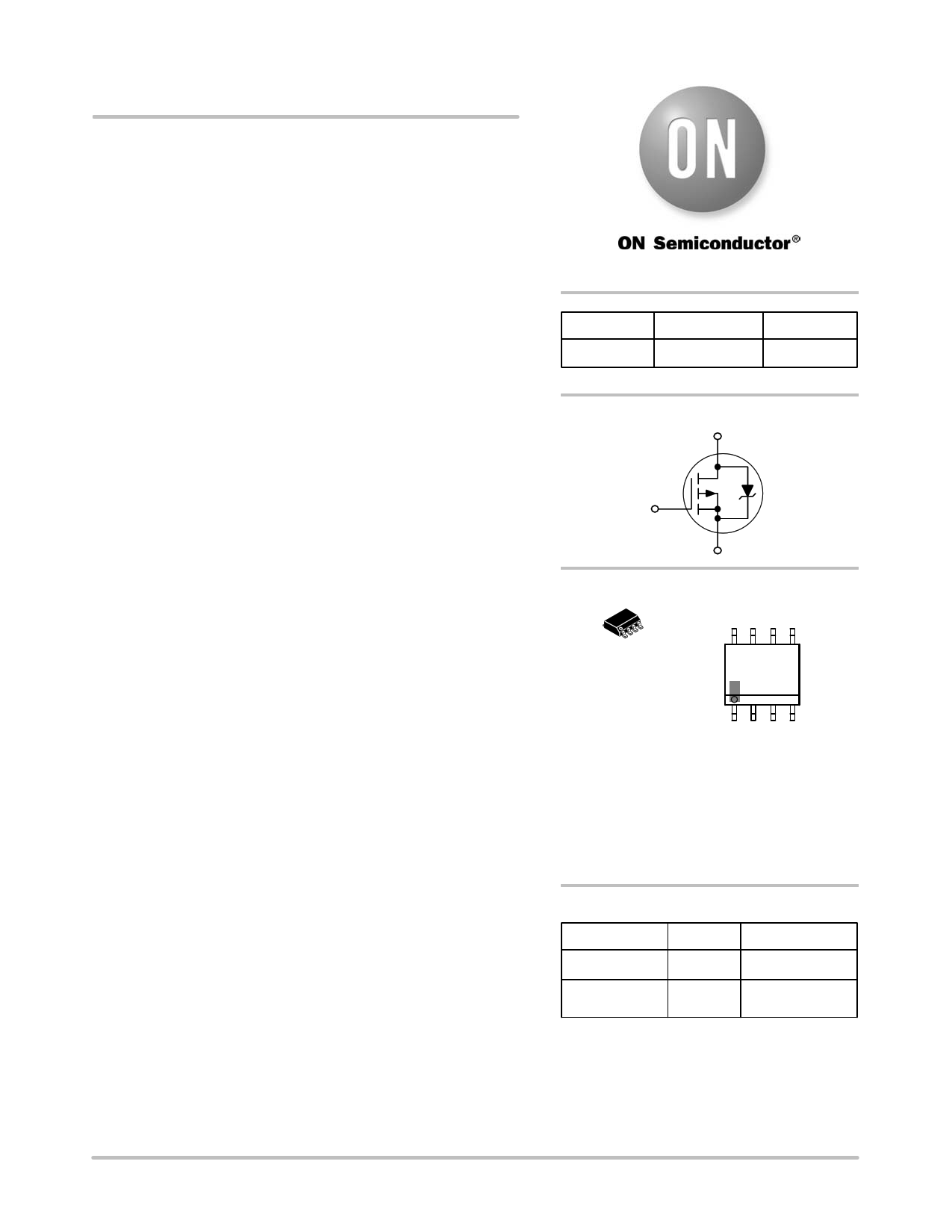
http://onsemi.com
VDSS
−20 V
RDS(ON) TYP
26 mW @ −4.5 V
ID MAX
−5.4 A
Single P−Channel
D
G
8
1
SOIC−8
CASE 751
STYLE 13
S
MARKING DIAGRAM &
PIN ASSIGNMENT
D D DD
8
E5P02x
AYWW G
G
1
NC S S G
E5P02 = Specific Device Code
x = Blank or S
A = Assembly Location
Y = Year
WW = Work Week
G = Pb−Free Package
(Note: Microdot may be in either location)
ORDERING INFORMATION
Device
NTMS5P02R2
NTMS5P02R2G
Package
Shipping†
SOIC−8 2500/Tape & Reel
SOIC−8 2500/Tape & Reel
(Pb−Free)
†For information on tape and reel specifications,
including part orientation and tape sizes, please
refer to our Tape and Reel Packaging Specifications
Brochure, BRD8011/D
© Semiconductor Components Industries, LLC, 2006
March, 2006 − Rev. 2
1
Publication Order Number:
NTMS5P02R2/D
1 page 
NTMS5P02R2
4000
VDS = 0 V
Ciss
VGS = 0 V
TJ = 25°C
3000
2000
Crss
1000
0
10
Crss
505
−VGS −VDS
Ciss
Coss
10 15
20
1000
100
GATE−TO−SOURCE OR
DRAIN−TO−SOURCE VOLTAGE (VOLTS)
Figure 7. Capacitance Variation
VDD = −16 V
ID = −5.4 A
VGS = −4.5 V
td(off)
tf
tr
td(on)
5
QT
4 −VDS
3 Q1
Q2
−VGS
20
16
12
28
ID = −5.4 A
1
TJ = 25°C
4
00
0 4 8 12 16 20 24
Qg, TOTAL GATE CHARGE (nC)
Figure 8. Gate−To−Source and Drain−To−Source
Voltage versus Total Charge
5 VGS = 0 V
TJ = 25°C
4
3
2
1
10
1 10 100
RG, GATE RESISTANCE (OHMS)
Figure 9. Resistive Switching Time Variation
versus Gate Resistance
0
0.2 0.3 0.4 0.5 0.6 0.7 0.8 0.9
1
−VSD, SOURCE−TO−DRAIN VOLTAGE (VOLTS)
Figure 10. Diode Forward Voltage versus Current
DRAIN−TO−SOURCE DIODE CHARACTERISTICS
100
VGS = 20 V
SINGLE PULSE
TC = 25°C
1 ms
10
10 ms
1
0.1
0.1
RDS(on) LIMIT
THERMAL LIMIT
PACKAGE LIMIT
dc
1 10 100
VDS, DRAIN−TO−SOURCE VOLTAGE (VOLTS)
Figure 11. Maximum Rated Forward Biased
Safe Operating Area
IS
tp
di/dt
trr
ta tb
0.25 IS
IS
TIME
Figure 12. Diode Reverse Recovery Waveform
http://onsemi.com
5
5 Page | ||
| Páginas | Total 7 Páginas | |
| PDF Descargar | [ Datasheet NTMS5P02R2.PDF ] | |
Hoja de datos destacado
| Número de pieza | Descripción | Fabricantes |
| NTMS5P02R2 | Power MOSFET ( Transistor ) | ON Semiconductor |
| NTMS5P02R2G | Power MOSFET ( Transistor ) | ON Semiconductor |
| Número de pieza | Descripción | Fabricantes |
| SLA6805M | High Voltage 3 phase Motor Driver IC. |
Sanken |
| SDC1742 | 12- and 14-Bit Hybrid Synchro / Resolver-to-Digital Converters. |
Analog Devices |
|
DataSheet.es es una pagina web que funciona como un repositorio de manuales o hoja de datos de muchos de los productos más populares, |
| DataSheet.es | 2020 | Privacy Policy | Contacto | Buscar |