|
|
|
PDF ZL50074 Data sheet ( Hoja de datos )
| Número de pieza | ZL50074 | |
| Descripción | 32 K x 32 K Channel TDM Switch | |
| Fabricantes | Zarlink Semiconductor | |
| Logotipo | ||
Hay una vista previa y un enlace de descarga de ZL50074 (archivo pdf) en la parte inferior de esta página. Total 30 Páginas | ||
|
No Preview Available !
ZL50074
32 K x 32 K Channel TDM Switch
with 128 Input and 128 Output Streams
Data Sheet
Features
January 2006
• 32,768 channel x 32,768 channel non-blocking
digital Time Division Multiplex (TDM) switch at
65.536 Mbps, 32.768 Mbps or 16.384 Mbps
• 16,384 channel x 16,384 channel non-blocking
digital TDM switch at 8.192 Mbps
• Up to 128 serial TDM input streams, divided into
32 groups with 4 input streams per group
• Up to 128 serial TDM output streams, divided into
32 groups with 4 output streams per group
• Per-group input bit delay for flexible sampling
point selection
• Per-group output fractional bit advancement
• Four sets of output timing signals for interfacing
additional devices
• Per-channel constant or variable throughput
delay for frame integrity and low latency
applications
Ordering Information
ZL50074GAC 484 Ball LBGA Trays
ZL50074GAG2 484 Ball PBGA** Trays
**Pb Free Tin/Silver/Copper
-40°C to +85°C
• Control interface compatible with Intel and
Motorola Selectable 32 bit and 16 bit non-
multiplexed buses
• Connection Memory block programming
• Supports ST-BUS and GCI-Bus standards for
input and output timing
• IEEE 1149.1 (JTAG) test port
• 3.3 V I/O with 5 V tolerant inputs; 1.8 V core
Applications
• Per-channel high impedance output control
• Large Switching Platforms
• Per-channel force-high output control
• Per-channel message mode
• Centralwww.DataSheet4U.com Office Switches
• Wireless Base Stations and Controllers
• Multi-service Access Platforms
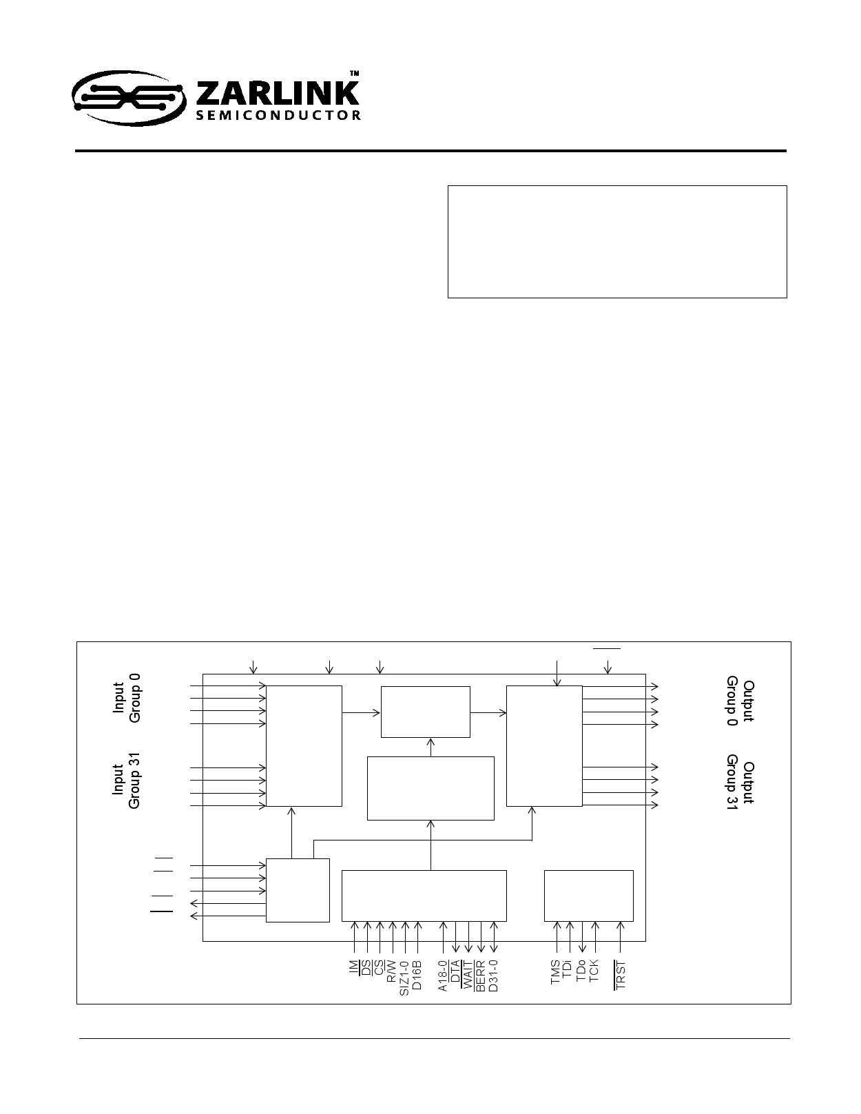
STiA0
STiB0
STiC0
STiD0
:
:
STiA31
STiB31
STiC31
STiD31
FPi2-0
CKi2-0
CK_SEL1-0
FPo3-0
CKo3-0
VDD_CORE VDD_IO VSS
ODE PWR
S/P
Converter
Input
Timing
Data Memory
P/S
Converter
Connection Memory
Output
Timing
Timing
Microprocessor Interface
and Control Registers
Test Access
Port
SToA0
SToB0
SToC0
SToD0
:
:
SToA31
SToB31
SToC31
SToD31
Figure 1 - ZL50074 Functional Block Diagram
1
Zarlink Semiconductor Inc.
Zarlink, ZL and the Zarlink Semiconductor logo are trademarks of Zarlink Semiconductor Inc.
Copyright 2004-2006, Zarlink Semiconductor Inc. All Rights Reserved.
1 page 
ZL50074
Data Sheet
List of Tables
Table 1 - Data Rate and Maximum Switch Size . . . . . . . . . . . . . . . . . . . . . . . . . . . . . . . . . . . . . . . . . . . . . . . . . . . 14
Table 2 - TDM Stream Bit Rates . . . . . . . . . . . . . . . . . . . . . . . . . . . . . . . . . . . . . . . . . . . . . . . . . . . . . . . . . . . . . . 15
Table 3 - CKi0 and FPi0 Setting via CK_SEL1 - 0 . . . . . . . . . . . . . . . . . . . . . . . . . . . . . . . . . . . . . . . . . . . . . . . . . 15
Table 4 - Example of Address and Byte Significance . . . . . . . . . . . . . . . . . . . . . . . . . . . . . . . . . . . . . . . . . . . . . . 21
Table 5 - 32 Bit Motorola Mode Byte Addressing . . . . . . . . . . . . . . . . . . . . . . . . . . . . . . . . . . . . . . . . . . . . . . . . . . 21
Table 6 - 32 Bit Motorola Mode Access Transfer Size . . . . . . . . . . . . . . . . . . . . . . . . . . . . . . . . . . . . . . . . . . . . . . 22
Table 7 - 32 Bit Intel Mode Bus Enable Signals . . . . . . . . . . . . . . . . . . . . . . . . . . . . . . . . . . . . . . . . . . . . . . . . . . . 22
Table 8 - Byte Enable Signals . . . . . . . . . . . . . . . . . . . . . . . . . . . . . . . . . . . . . . . . . . . . . . . . . . . . . . . . . . . . . . . . 23
Table 9 - 16 Bit Mode Word Alignment. . . . . . . . . . . . . . . . . . . . . . . . . . . . . . . . . . . . . . . . . . . . . . . . . . . . . . . . . . 23
Table 10 - 16 Bit Mode Example Byte Address . . . . . . . . . . . . . . . . . . . . . . . . . . . . . . . . . . . . . . . . . . . . . . . . . . . 24
Table 11 - Memory Map . . . . . . . . . . . . . . . . . . . . . . . . . . . . . . . . . . . . . . . . . . . . . . . . . . . . . . . . . . . . . . . . . . . . . 29
Table 12 - Connection Memory Group Address Mapping . . . . . . . . . . . . . . . . . . . . . . . . . . . . . . . . . . . . . . . . . . . 30
Table 13 - Connection Memory Stream Address Offset at Various Output Rates . . . . . . . . . . . . . . . . . . . . . . . . . 30
Table 14 - Connection Memory Timeslot Address Offset Range . . . . . . . . . . . . . . . . . . . . . . . . . . . . . . . . . . . . . . 31
Table 15 - Connection Memory Bits (CMB) . . . . . . . . . . . . . . . . . . . . . . . . . . . . . . . . . . . . . . . . . . . . . . . . . . . . . . 32
Table 16 - Connection Memory LSB Group Address Mapping . . . . . . . . . . . . . . . . . . . . . . . . . . . . . . . . . . . . . . . 33
Table 17 - Connection Memory LSB Stream Address Offset at Various Output Rates . . . . . . . . . . . . . . . . . . . . . 34
Table 18 - Data Memory Group Address Mapping. . . . . . . . . . . . . . . . . . . . . . . . . . . . . . . . . . . . . . . . . . . . . . . . . 34
Table 19 - Data Memory Stream Address Offset at Various Output Rates . . . . . . . . . . . . . . . . . . . . . . . . . . . . . . 35
Table 20 - Group Control Register Addressing . . . . . . . . . . . . . . . . . . . . . . . . . . . . . . . . . . . . . . . . . . . . . . . . . . . 36
Table 21 - Group Control Register . . . . . . . . . . . . . . . . . . . . . . . . . . . . . . . . . . . . . . . . . . . . . . . . . . . . . . . . . . . . . 36
Table 22 - Input Clock Control Register . . . . . . . . . . . . . . . . . . . . . . . . . . . . . . . . . . . . . . . . . . . . . . . . . . . . . . . . . 39
Table 23 - Output Clock Control Register . . . . . . . . . . . . . . . . . . . . . . . . . . . . . . . . . . . . . . . . . . . . . . . . . . . . . . . 40
Table 24 - Block and Power-up Initialization Status Bits . . . . . . . . . . . . . . . . . . . . . . . . . . . . . . . . . . . . . . . . . . . . 44
5
Zarlink Semiconductor Inc.
5 Page 
ZL50074
Data Sheet
Pin Description (continued)
Pin Name
Description
A1, AB4, R18, E14
G5, Y6, T19, C17
CKo0-3
FPo0-3
ST-BUS/GCI-Bus Clock Outputs (3.3 V Outputs with Slew-Rate
Control)
These clock outputs can be programmed to generate 8.192 MHz,
16.384 MHz, 32.678 MHz or 65.536 MHz TDM clock outputs. The
active edge can be programmed to be either rising or falling. The
source of the clock outputs can be derived from either the CKi2-0
inputs or the internal system clock. The frequency, active edge and
source of each clock output can be programmed independently by
the Output Clock Control Register (Section 12.5). For 65.536 MHz
output clock, the total loading on the output should not be
larger than 10pF.
ST-BUS/GCI-Bus Frame Pulse Outputs (3.3 V Outputs with
Slew-Rate Control)
These 8 kHz output pulses mark the frame boundary of the TDM
data streams. The pulse width is nominally one clock period of the
corresponding CKo output. The active state of each frame pulse
may be either high or low, independently programmed by the
Output Clock Control Register (Section 12.5).
W15, V14
L1
A18, J21, M22, R3, V13,
W13, Y13, AA16, AA17
AB13, AB14
CK_SEL0-1
Master Clock Input Select (5 V Tolerant Inputs)
Inputs used to select the frequency and frame alignment of CKi0
and FPi0:
CK_SEL1 = 0, CK_SEL0 = 0, 8.192 MHz
CK_SEL1 = 0, CK_SEL0 = 1, 16.384 MHz
CK_SEL1 = 1, CK_SEL0 = 0, 32.768 MHz
CK_SEL1 = 1, CK_SEL0 = 1, 65.536 MHz
ODE
Output Drive Enable (5 V Tolerant Input with Internal Pull-up)
This is the asynchronous output enable control for the output
streams. When it is high, the streams are enabled. When it is low,
the output streams are tristated.
IC Internal Connections
In normal mode these pins MUST be connected low
NC No Connection
In normal mode these pins MUST be left unconnected.
Microprocessor Port and Reset
A11, C11, E11, B11, A10,
B10, C10, A9, D10, B9, F11,
A8, C9, B8, E10, A7, A6, D9,
E9, C8, A5, B6, C7, D8, E8,
A4, B5, C6, D7, F8, A3, B4
B16, A17, A16, C14, E13,
D13, B15, A15, B14, C13,
A14, B13, E12, D12, A13,
C12, D11, B12, A12
C16
D0-31
A0-18
CS
Microprocessor Port Data Bus (5 V Tolerant Bi-directional with
Slew-Rate Output Control)
32 or 16 bit bidirectional data bus. Used for microprocessor access
to internal memories and registers. When 16 bit mode is selected
(D16B is logic 1), D31-16 are unused and must be connected to
defined logic levels.
Microprocessor Port Address Bus (5 V Tolerant Inputs)
19 bit address bus for the internal memories and registers. In 16 bit
bus mode (D16B is logic 1), please note A0 is not used and must
be connected to a defined logic level.
In Intel 32 bit mode: A1 = BE3, A0 = BE2
Chip Select Input (5 V Tolerant Input)
Active low input used with DS to enable read and write access to
the ZL50074.
11
Zarlink Semiconductor Inc.
11 Page | ||
| Páginas | Total 30 Páginas | |
| PDF Descargar | [ Datasheet ZL50074.PDF ] | |
Hoja de datos destacado
| Número de pieza | Descripción | Fabricantes |
| ZL50070 | 24 K Channel Digital Switch | Zarlink Semiconductor |
| ZL50073 | 32 K Channel Digital Switch | Zarlink Semiconductor |
| ZL50074 | 32 K x 32 K Channel TDM Switch | Zarlink Semiconductor |
| ZL50075 | 32 K Channel Digital Switch | Zarlink Semiconductor |
| Número de pieza | Descripción | Fabricantes |
| SLA6805M | High Voltage 3 phase Motor Driver IC. |
Sanken |
| SDC1742 | 12- and 14-Bit Hybrid Synchro / Resolver-to-Digital Converters. |
Analog Devices |
|
DataSheet.es es una pagina web que funciona como un repositorio de manuales o hoja de datos de muchos de los productos más populares, |
| DataSheet.es | 2020 | Privacy Policy | Contacto | Buscar |