|
|
|
PDF UT9Q512K32 Data sheet ( Hoja de datos )
| Número de pieza | UT9Q512K32 | |
| Descripción | 16Megabit SRAM MCM | |
| Fabricantes | AEROFLEX | |
| Logotipo | ||
Hay una vista previa y un enlace de descarga de UT9Q512K32 (archivo pdf) en la parte inferior de esta página. Total 14 Páginas | ||
|
No Preview Available !
www.DataSheet4U.com
Standard Products
QCOTSTM UT9Q512K32 16Megabit SRAM MCM
Data Sheet
June, 2003
FEATURES
q 25ns maximum (5 volt supply) address access time
q Asynchronous operation for compatible with industry
standard 512K x 8 SRAMs
q TTL compatible inputs and output levels , three-state
bidirectional data bus
q Typical radiation performance
- Total dose: 50krads
- SEL Immune >80 MeV-cm2/mg
- LETTH(0.25) = >10 MeV-cm2/mg
- Saturated Cross Section (cm2) per bit, 5.0E -9
- <1E-8 errors/bit-day, Adams 90% geosynchronous
heavy ion
q Packaging options:
- 68-lead dual cavity ceramic quad flatpack (CQFP) -
(weight 7.37 grams)
q Standard Microcircuit Drawing 5962-01511
- QML T and Q compliant part
INTRODUCTION
The QCOTSTM UT9Q512K32 Quantified Commercial
Off-the-Shelf product is a high-performance 2M byte
(16Mbit) CMOS static RAM multi-chip module (MCM),
organized as four individual 524,288 x 8 bit SRAMs with a
common output enable. Memory expansion is provided by
an active LOW chip enable (En), an active LOW output
enable (G), and three-state drivers. This device has a power-
down feature that reduces power consumption by more than
90% when deselected.
Writing to each memory is accomplished by taking chip
enable (En) input LOW and write enable ( Wn) inputs LOW.
Data on the eight I/O pins (DQ0 through DQ7) is then written
into the location specified on the address pins (A0 through
A18). Reading from the device is accomplished by taking
chip enable (En) and output enable ( G) LOW while forcing
write enable (Wn) HIGH. Under these conditions, the
contents of the memory location specified by the address
pins will appear on the I/O pins.
The input/output pins are placed in a high impedance state
when the device is deselected (En HIGH), the outputs are
disabled (G HIGH), or during a write operation (En LOW
and Wn LOW). Perform 8, 16, 24 or 32 bit accesses by
making Wn along with En a common input to any
combination of the discrete memory die.
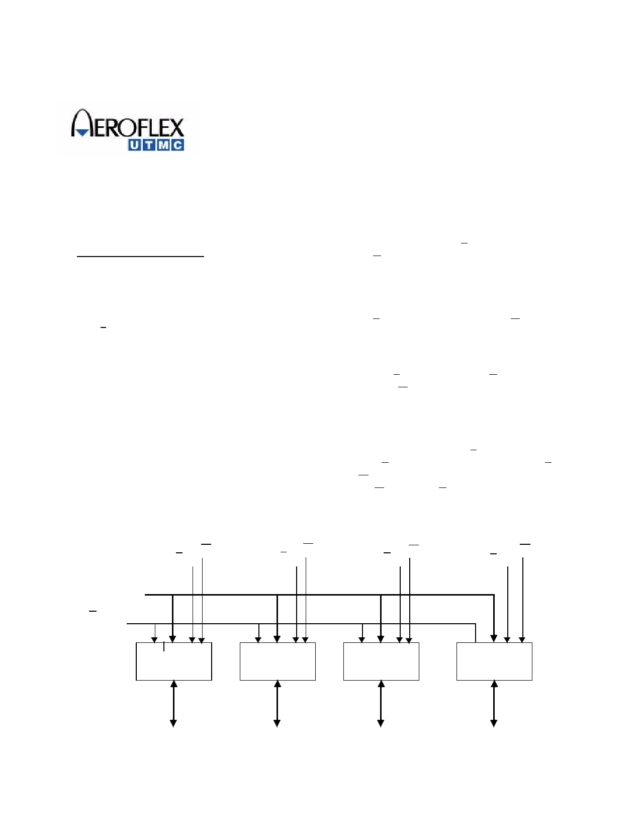
A(18:0)
G
W3
E3
512K x 8
W2
E2
512K x 8
W1
E1
512K x 8
W0
E0
512K x 8
DQ(31:24)
or
DQ3(7:0)
DQ(23:16)
or
DQ2(7:0)
DQ(15:8)
or
DQ1(7:0)
Figure 1. UT9Q512K32 SRAM Block Diagram
DQ(7:0)
or
DQ0(7:0)
1 page 
DC ELECTRICAL CHARACTERISTICS (Pre/Post-Radiation)*
(-40°C to +125°C) (VDD = 5.0V + 10%)
SYMBOL
PARAMETER
CONDITION
MIN
VIH High-level input voltage
VIL Low-level input voltage
2.0
VOL1
VOL2
VO H 1
VO H 2
CIN1
CIO1
IIN
IOZ
Low-level output voltage
Low-level output voltage
High-level output voltage
High-level output voltage
Input capacitance
IOL = 8mA, VDD =4.5V
IOL = 200µA,VDD =4.5V
IOH = -4mA,VDD =4.5V
IOH = 200µA,VDD =4.5V
ƒ = 1MHz @ 0V
Bidirectional I/O capacitance
ƒ = 1MHz @ 0V
Input leakage current
Three-state output leakage current
VIN = VDD and VSS, VDD = VDD (max)
VO = VDD and VSS
VDD = VDD (max)
G = VDD (max)
2.4
3.0
-2
-2
IOS2, 3 Short-circuit output current
IDD(OP)
Supply current operating
@ 1MHz
(per byte)
I D D 1( O P )
Supply current operating
@40MHz
(per byte)
ID D2 (SB)
Supply current standby
@0MHz
(per byte)
VDD = VDD (max), VO = VDD
VDD = VDD (max), VO = 0V
Inputs: VIL = 0.8V,
VIH = 2.0V
IOUT = 0mA
VDD = VDD (max)
Inputs: VIL = 0.8V,
VIH = 2.0V
IOUT = 0mA
VDD = VDD (max)
Inputs: VIL = VSS
IOUT = 0mA
E1 = VDD - 0.5, VDD = VDD (max)
VIH = VDD - 0.5V
-90
-40°C and
25°C
125°C
Notes:
* Post-radiation performance guaranteed at 25°C per MIL-STD-883 Method 1019 .
1. Measured only for initial qualification and after process or design changes that could affect input/output capacitance.
2. Supplied as a design limit but not guaranteed or tested.
3. Not more than one output may be shorted at a time for maximum duration of one second.
MAX
0.8
0.4
0.08
32
16
2
2
90
125
180
6
12
UNIT
V
V
V
V
V
V
pF
pF
µA
µA
mA
mA
mA
mA
mA
5
5 Page 
VDD
E1
DATA RETENTION MODE
4. 5V
VDR > 2.5V
tEFR
4.5V
tR
VDD =VDR
Figure 7. Low VDD Data Retention Waveform
DATA RETENTION CHARACTERISTICS (Pre/Post-Irradiation)
(1 Second Data retention Test)
SYMBOL
PARAMETER
VDR VDD for data retention
IDDR 1,2
Data retention current (per byte)
tEFR 1,3
Chip deselect to data retention time
tR1,3 Operation recovery time
Notes:
1. En = VDD - .2V, all other inputs = V DR or VSS.
2. Data retention current (ID D R) Tc = 25oC.
3. Not guaranteed or tested.
4. VDR = T=-40 oC and 125 oC.
DATA RETENTION CHARACTERISTICS (Pre/Post-Irradiation)
(10 Second Data Retention Test, TC=-40oC and +125oC)
SYMBOL
PARAMETER
V DD 1
VDD for data retention
tEFR2, 3
Chip select to data retention time
tR2, 3
Operation recovery time
MINIMUM
2.5
--
0
tAVAV
MAXIMUM UNIT
-- V
5.0 mA
ns
Ns
MINIMUM
4.5
0
tAVAV
MAXIMUM UNIT
5.5 V
ns
ns
Notes:
1. Performed at VDD (min) and VDD (max).
2. En = VSS, all other inputs = V DR or V SS.
3. Not guaranteed or tested.
11
11 Page | ||
| Páginas | Total 14 Páginas | |
| PDF Descargar | [ Datasheet UT9Q512K32.PDF ] | |
Hoja de datos destacado
| Número de pieza | Descripción | Fabricantes |
| UT9Q512K32 | 16Megabit SRAM MCM | AEROFLEX |
| UT9Q512K32 | 16Megabit SRAM MCM | Aeroflex Circuit Technology |
| UT9Q512K32E | 16 Megabit RadTolerant SRAM MCM | Aeroflex Circuit Technology |
| Número de pieza | Descripción | Fabricantes |
| SLA6805M | High Voltage 3 phase Motor Driver IC. |
Sanken |
| SDC1742 | 12- and 14-Bit Hybrid Synchro / Resolver-to-Digital Converters. |
Analog Devices |
|
DataSheet.es es una pagina web que funciona como un repositorio de manuales o hoja de datos de muchos de los productos más populares, |
| DataSheet.es | 2020 | Privacy Policy | Contacto | Buscar |