|
|
|
PDF XC9511 Data sheet ( Hoja de datos )
| Número de pieza | XC9511 | |
| Descripción | Synchronous Step-Down DC/DC Converter | |
| Fabricantes | Torex Semiconductor | |
| Logotipo | ||
Hay una vista previa y un enlace de descarga de XC9511 (archivo pdf) en la parte inferior de esta página. Total 13 Páginas | ||
|
No Preview Available !
www.DataSheet4U.com
XC9511 Series
February 2, 2004 V5
Synchronous Step-Down DC/DC Converter with built-in LDO Regulator in parallel plus Voltage Detector
Preliminary
! Synchronous step-down DC/DC converter
with built-in LDO regulator plus voltage detector
! Step-down DC/DC converter's output connected in parallel
with LDO regulator
! SOP-8 package for high current
! Small-footprint
! Output Current (DC/DC : 800mA, VR : 400mA)
! Ceramic capacitor compatible (Low ESR capacitors)
! APPLICATIONS
" CD-R / RW, DVD
" HDD
" PDAs, portable communication modem
" Cellular phones
" Palmtop computers
" Cameras, video recorders
! GENERAL DESCRIPTION
The XC9511 series consists of a step-down DC/DC converter and a
high-speed LDO regulator connected in parallel with the DC/DC
converter's output. A voltage detector is also built-in. Since the input
for the LDO voltage regulator block comes from the input power
supply, it is suited for use with various applications.
The DC/DC converter block incorporates a P-Channel driver transistor
and a synchronous N-Channel switching transistor. With an external
coil, diode and two capacitors, the XC9511 can deliver output currents
up to 800mA at efficiencies over 90%. The XC9511 is designed for
use with small ceramic capacitors.
A choice of three switching frequencies are available, 300 kHz,
600 kHz, and 1.2 MHz.
Output voltage settings for the DC/DC and VR are set-up internally in
100mV steps within the range of 0.9V to 4.0V (± 2.0%). For the VD,
the range is of 0.9V to 5.0V (± 2.0%).
The soft start time of the series is internally set to 5ms. With the built-
in U.V.L.O. (Under Voltage Lock Out) function, the internal P-channel
driver transistor is forced OFF when input voltage becomes 1.4 V or
lower.
! FEATURES
Input Voltage Range : 2.4V ~ 6.0V
Load Capacitors :
Ceramic Capacitor Compatible
(Low ESR Capacitors)
VD Function :
Detects output voltage from the VDOUT pin
while sensing either VDD, DCOUT,
or VROUT internally.
Nch Open Drain Output
<DC/DC Converter>
Output Voltage Range : 0.9V ~ 4.0V (Accuracy ±2%)
Output Current :
800mA
Controls :
PWM Control
PWM, PWM / PFM Automatic
Switching External
Oscillation Frequency : 300kHz, 600kHz, 1.2MHz
<Regulator>
Output Voltage Range : 0.9V ~ 4.0V (Accuracy ±2%)
Current Limit
600mA
Dropout Voltage :
160mV @ IOUT=200mA (VOUT=2.8V)
High Ripple Rejection 60dB @1kHz (VOUT=2.8V)
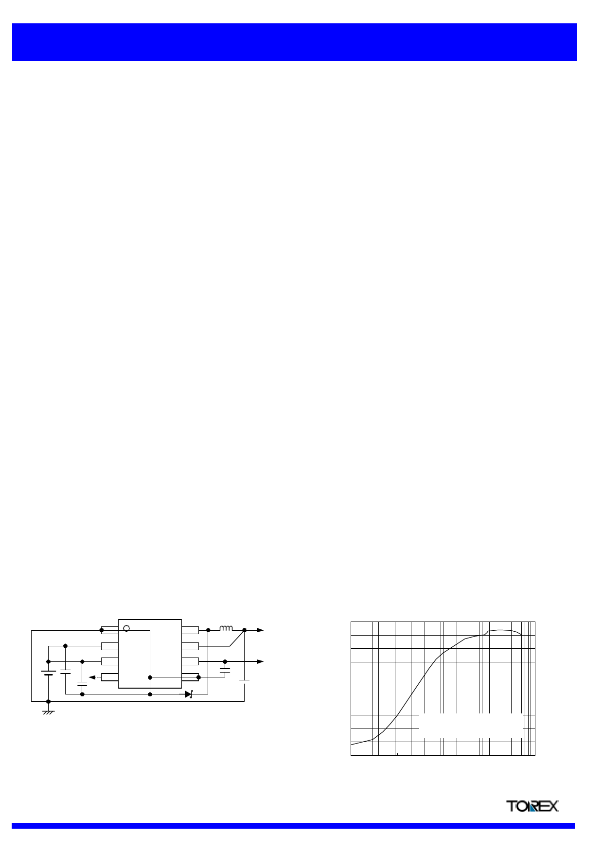
! TYPICAL APPLICATION CIRCUIT
1
PGND
2 PVDD
LX 8
DCOUT 7
+
CIN1
+
CIN2
3 AVDD
VROUT 6
4 VDOUT
AGND
5
()
SD
SOP-8 (TOP VIEW)
L
DCOUT
+
C L2
VROUT
+
C L1
! TYPICAL PERFORMANCE CHARACTERISTICS
XC9511Axxxx
VIN=5.0V, Topr=25OC, L:4.7uH(CDRH4D28C)
CIN:4.7uF(ceramic), CL1:10uF(ceramic), CL2:1uF(ceramic)
100
90
80
70
60
50
40
30
DC/DC Efficiency
20 (DCOUT:3.3V, 1.2MHz)
10
0
0.1 1 10 100 1000
DC/DC Output Current IDOUT
Data Sheet
Semiconductor Ltd.
1
1 page 
XC9511 Series
Synchronous Step-Down DC/DC Converter with built-in LDO Regulator in parallel plus Voltage Detector
Preliminary
! ELECTRICAL CHARACTERISTICS (Continued)
# Detector (2.7V product)
PARAMETER
SYMBOL
CONDITIONS
Detect Voltage
Hysteresis Range
VDF(E)
VHYS
CE=0V
VHYS=[VDR(E) (note 10) - VDF(E)]
VDF(E) x 100
VD Output Current
Output Voltage
Temperature Characteristics
IVD
! VDF
(! Topr " VDF)
VDOUT=0.5V, CE=0V
CE=0V,
-40OC<Topr<85OC
Test Conditions : Unless otherwise stated;
DC/DC : VIN=3.6V [@ DCOUT:1.5V]
VR : VIN = 4.3V (VIN=VROUT(T) + 1.0V)
VD : VIN=6.0V
Common conditions for all test items : CE=VIN, MODE=0V
* VROUT(T) : Setting Output Voltage
MIN.
2.646
2
1
-
TYP.
2.700
5
-
±100
MAX.
2.754
8
-
-
UNITS
Topr=25OC
TEST
CIRCUIT
V8
%8
mA
ppm/OC
9
8
note 1: Including hysteresis operating voltage range.
note 2: ON resistance (Ω)= 0.05 (V) / ILX (A)
note 3: EFFI = { ( Output Voltage x Output Current ) / ( Input Voltage x Input Current) } x 100
note 4: Time until it short-circuits DCOUT with GND through 1Ω of resistance from a state of operation
and is set to DCOUT=0V from current limit pulse generating.
note 5: Vdif = (VIN1 (note 6) - VROUT1 (note 7 ) )
note 6: VIN 1 = The input voltage when VROUT1 appears as input voltage is gradually decreased.
note 7: VROUT1 = A voltage equal to 98% of the output voltage whenever an amply stabilized IOUT {VROUT(T) + 1.0V} is input.
note 8: Current limit = When VIN is low, limit current may not be reached because of voltage falls caused
by ON resistance or serial resistance of coils.
note 9: Integral latch circuit=latch time may become longer and latch operation may not work when VIN is 3.0V or more.
note 10 : VDR(E) = VD release voltage
note 11 : When temperature is high, a current of approximately 5.0µA (maximum) may leak.
note 12 : When using the IC with a regulator output at almost no load, a capacitor should be placed as close as possible between
AVDD and AGND (CIN2), connected with low impedance. Please also see the recommended pattern layout
on page 13 for your reference. Should it not be possible to place the input capacitor nearby, the regulated output level
may increase up to the VDD level while the load of the DC/DC converter increases and the regulator output is at almost no load.
Semiconductor Ltd.
Data Sheet
5
5 Page 
XC9511 Series
Synchronous Step-Down DC/DC Converter with built-in LDO Regulator in parallel plus Voltage Detector
Preliminary
! NOTES ON USE
" Application Information
1. The XC9511 series is designed for use with a ceramic output capacitor. If, however, the potential difference between dropout voltage or
output current is too large, a ceramic capacitor may fail to absorb the resulting high switching energy and oscillation could occur on the
output. If the input-output potential difference is large, connect an electrolytic capacitor in parallel to compensate for insufficient
capacitance.
2. Spike noise and ripple voltage arise in a switching regulator as with a DC/DC converter. These are greatly influenced by external
component selection, such as the coil inductance, capacitance values, and board layout of external components. Once the design has
been completed, verification with actual components should be done.
3. When the difference between VIN and VOUT is large in PWM control, very narrow pulses will be outputted, and there is the possibility
that some cycles may be skipped completely.
4. When the difference between VIN and VOUT is small, and the load current is heavy, very wide pulses will be outputted and there is the
possibility that some cycles may be skipped completely: in this case, the Lx pin may not go low at all.
# DC/DC Waveform (3.3V, 1.2MHz)
CH1:LX
CH1:LX
CH2:DCOUT
Off-set Voltage:3.3V
CH2:DCOUT
Off-set Voltage:3.3V
VIN=3.7V, IDOUT=100mA
<External Components>
L: 4.7µH (CDRH4D28C, SUMIDA)
CIN: 4.7µF (ceramic)
CL: 10µF (ceramic)
VIN=3.5V, IDOUT=100mA
<External Components>
L: 4.7µH (CDRH4D28C, SUMIDA)
CIN: 4.7µF (ceramic)
CL: 10µF (ceramic)
5. The IC's DC/DC converter operates in synchronous mode when the coil current is in a continuous state and non-synchronous mode when
the coil current is in a discontinuous state. In order to maintain the load current value when synchronous switches to non-synchronous and
vise versa, a ripple voltage may increase because of the repetition of switching between synchronous and non-synchronous. When this
state continues, the increase in the ripple voltage stops. To reduce the ripple voltage, please increase the load capacitance value or use a
schottky diode externally. When the current used becomes close to the value of the load current when synchronous switches to non-
synchronous and vise versa, the switching current value can be changed by changing the coil inductance value. In case changes to coil
inductance are to values other than the recommended coil inductance values, verification with actual components should be done.
Ics= (VIN - DCOUT) x OnDuty / (L x Fosc)
Ics : Switching current from synchronous rectification to non-synchronous rectification
OnDuty : OnDuty ratio of P-ch driver transistor ( step down ratio : DCOUT / VIN)
L : Coil inductance value
Fosc : Oscillation Frequency
IDOUT : The DC/DC load current
Data Sheet
11
Semiconductor Ltd.
11 Page | ||
| Páginas | Total 13 Páginas | |
| PDF Descargar | [ Datasheet XC9511.PDF ] | |
Hoja de datos destacado
| Número de pieza | Descripción | Fabricantes |
| XC9510 | Synchronous Step-Down DC/DC Converter with Built-In LDO Regulator In Series plus Voltage Detector | Torex Semiconductor |
| XC95103SL | Synchronous Step-Down DC/DC Converter with Built-In LDO Regulator In Series plus Voltage Detector | Torex Semiconductor |
| XC95103SR | Synchronous Step-Down DC/DC Converter with Built-In LDO Regulator In Series plus Voltage Detector | Torex Semiconductor |
| XC95106SL | Synchronous Step-Down DC/DC Converter with Built-In LDO Regulator In Series plus Voltage Detector | Torex Semiconductor |
| Número de pieza | Descripción | Fabricantes |
| SLA6805M | High Voltage 3 phase Motor Driver IC. |
Sanken |
| SDC1742 | 12- and 14-Bit Hybrid Synchro / Resolver-to-Digital Converters. |
Analog Devices |
|
DataSheet.es es una pagina web que funciona como un repositorio de manuales o hoja de datos de muchos de los productos más populares, |
| DataSheet.es | 2020 | Privacy Policy | Contacto | Buscar |