|
|
|
PDF ADC12DS080 Data sheet ( Hoja de datos )
| Número de pieza | ADC12DS080 | |
| Descripción | (ADC12DSxxx) A/D Converter | |
| Fabricantes | National Semiconductor | |
| Logotipo | ||
Hay una vista previa y un enlace de descarga de ADC12DS080 (archivo pdf) en la parte inferior de esta página. Total 30 Páginas | ||
|
No Preview Available !
www.DataSheet4U.com
ADVANCE INFORMATION
February 2007
ADC12DS065/ADC12DS080/ADC12DS095/ADC12DS105
Dual 12-Bit, 65/80/95/105 MSPS A/D Converter with Serial
LVDS outputs
General Description
NOTE: This is Advance Information for products current-
ly in development. ALL specifications are design targets
and are subject to change.
The ADC12DS065, ADC12DS080, ADC12DS095, and AD-
C12DS105 are high-performance CMOS analog-to-digital
converters capable of converting two analog input signals into
12-bit digital words at rates up to 65/80/95/105 Mega Samples
Per Second (MSPS) respectively. The digital outputs are se-
rialized and provided on differential LVDS signal pairs. These
converters use a differential, pipelined architecture with digital
error correction and an on-chip sample-and-hold circuit to
minimize power consumption and the external component
count, while providing excellent dynamic performance. A
unique sample-and-hold stage yields a full-power bandwidth
of 1 GHz. The ADC12DS065/080/095/105 may be operated
from a single +3.3V power supply and consumes low power.
A power-down feature reduces the power consumption to
very low levels while still allowing fast wake-up time to full
operation. The differential inputs provide a 2V full scale dif-
ferential input swing. A stable 1.2V internal voltage reference
is provided, or the ADC12DS065/080/095/105 can be oper-
ated with an external 1.2V reference. Output data format
(offset binary versus 2's complement) and duty cycle stabi-
lizer are pin-selectable. The duty cycle stabilizer maintains
performance over a wide range of clock duty cycles.
The ADC12DS065/080/095/105 is available in a 60-lead LLP
package and operates over the industrial temperature range
of −40°C to +85°C.
Features
■ 1 GHz Full Power Bandwidth
■ Internal sample-and-hold circuit and precision reference
■ Low power consumption
■ Clock Duty Cycle Stabilizer
■ Single +3.3V supply operation
■ Offset binary or 2's complement output data format
■ Serial LVDS Outputs
■ 60-pin LLP package, (9x9x0.8mm, 0.5mm pin-pitch)
Key Specifications
■ For ADC12DS105
■ Resolution
■ Conversion Rate
■ SNR (fIN = 240 MHz)
■ SFDR (fIN = 240 MHz)
■ Full Power Bandwidth
■ Power Consumption
12 Bits
105 MSPS
67 dBFS (typ)
83 dBFS (typ)
1 GHz (typ)
1060 mW (typ)
Applications
■ High IF Sampling Receivers
■ Wireless Base Station Receivers
■ Test and Measurement Equipment
■ Communications Instrumentation
■ Portable Instrumentation
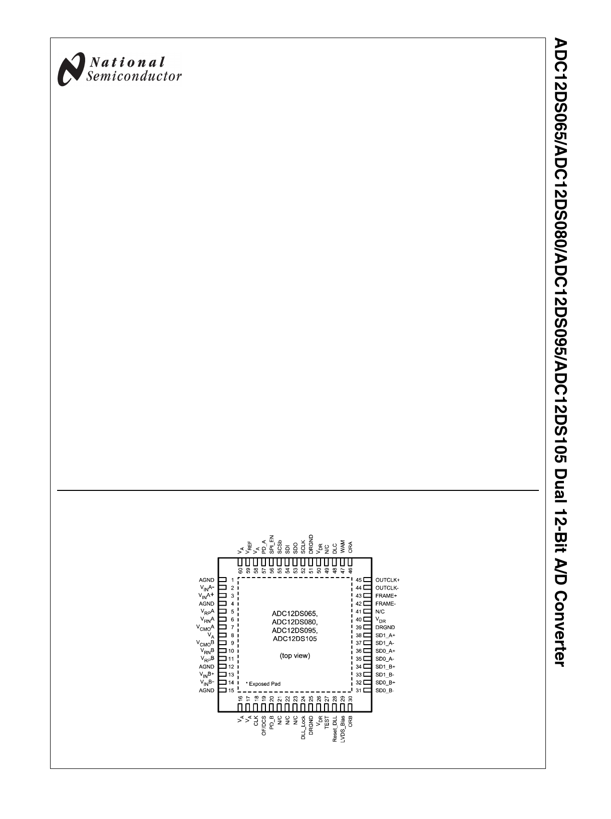
Connection Diagram
© 2007 National Semiconductor Corporation 202117
20211701
www.national.com
1 page 
Pin No.
Symbol
38 SD1_A+
37 SD1_A-
34 SD1_B+
33 SD1_B-
36 SD0_A+
35 SD0_A-
32 SD0_B+
31 SD0_B-
56 SPI_EN
55 SCSb
52 SCLK
54 SDI
Equivalent Circuit
Description
Serial Data Output 1 for Channel A. This is a differential LVDS pair
of signals that carries channel A ADC’s output in serialized form.
The serial data is provided synchronous with the OUTCLK output.
In Single-Lane mode each sample’s output is provided in
succession. In Dual-Lane mode every other sample output is
provided on this output. This differential output is always enabled
while the device is powered up. In power-down mode this output
holds the last logic state. A 100-ohm termination resistor must
always be used between this pair of signals at the far end of the
transmission line.
Serial Data Output 1 for Channel B. This is a differential LVDS pair
of signals that carries channel B ADC’s output in serialized form.
The serial data is provided synchronous with the OUTCLK output.
In Single-Lane mode each sample’s output is provided in
succession. In Dual-Lane mode every other sample output is
provided on this output. This differential output is always enabled
while the device is powered up. In power-down mode this output
holds the last logic state. A 100-ohm termination resistor must
always be used between this pair of signals at the far end of the
transmission line.
Serial Data Output 0 for Channel A. This is a differential LVDS pair
of signals that carries channel A ADC’s alternating samples’ output
in serialized form in Dual-Lane mode. The serial data is provided
synchronous with the OUTCLK output. In Single-Lane mode this
differential output is held in high impedance state. This differential
output is always enabled while the device is powered up. In power-
down mode this output holds the last logic state. A 100-ohm
termination resistor must always be used between this pair of
signals at the far end of the transmission line.
Serial Data Output 0 for Channel B. This is a differential LVDS pair
of signals that carries channel B ADC’s alternating samples’ output
in serialized form in Dual-Lane mode. The serial data is provided
synchronous with the OUTCLK output. In Single-Lane mode this
differential output is held in high impedance state. This differential
output is always enabled while the device is powered up. In power-
down mode this output holds the last logic state. A 100-ohm
termination resistor must always be used between this pair of
signals at the far end of the transmission line.
SPI Enable: The SPI interface is enabled when this signal is
asserted high. In this case the direct control pins have no effect.
When this signal is deasserted, the SPI interface is disabled and
the direct control pins are enabled.
Serial Chip Select: While this signal is asserted SCLK is used to
accept serial data present on the SDI input and to source serial
data on the SDO output. When this signal is deasserted, the SDI
input is ignored and the SDO output is in tri-state mode.
Serial Clock: Serial data are shifted into and out of the device
synchronous with this clock signal.
Serial Data-In: Serial data are shifted into the device on this pin
while SCSb signal is asserted.
5 www.national.com
5 Page 
ADC12DS080 Converter Electrical Characteristics
This product is currently under development. As such, the parameters specified are DESIGN TARGETS. The specifica-
tions cannot be guaranteed until device characterization has taken place.
Unless otherwise specified, the following specifications apply: AGND = DRGND = 0V, VA = VDR = +3.0V, Internal VREF = +1.2V,
fCLK = 80 MHz, VCM = VCMO, CL = 5 pF/pin. Typical values are for TA = 25°C. Boldface limits apply for TMIN ≤ TA ≤ TMAX. All other
limits apply for TA = 25°C (Notes 8, 9)
Symbol
Parameter
Conditions
Typical
(Note 10)
Limits
Units
(Limits)
STATIC CONVERTER CHARACTERISTICS
Resolution with No Missing Codes
12 Bits (min)
INL Integral Non Linearity (Note 11)
LSB (max)
±0.5
LSB (min)
DNL
Differential Non Linearity
±0.25
LSB (max)
LSB (min)
Under Range Output Code
00
Over Range Output Code
4095 4095
REFERENCE AND ANALOG INPUT CHARACTERISTICS
VCMO
Common Mode Output Voltage
1.45
1.5 1.55
V (min)
V (max)
VCM Analog Input Common Mode Voltage
1.5
1.4
1.6
V (min)
V (max)
CIN
VIN Input Capacitance (each pin to
GND) (Note 12)
VIN = 1.5 Vdc
± 0.5 V
(CLK LOW)
(CLK HIGH)
8.5
3.5
pF
pF
VREF
External Reference Voltage
1.20
1.176
1.224
V (min)
V (max)
ADC12DS080 Dynamic Converter Electrical Characteristics
Unless otherwise specified, the following specifications apply: AGND = DRGND = 0V, VA = VDR = +3.0V, Internal VREF = +1.2V,
fCLK = 80 MHz, VCM = VCMO, CL = 5 pF/pin, . Typical values are for TA = 25°C. Boldface limits apply for TMIN ≤ TA ≤ TMAX. All
other limits apply for TA = 25°C (Notes 8, 9)
Symbol
Parameter
Conditions
Typical
(Note 10) Limits
Units
(Limits)
(Note 2)
DYNAMIC CONVERTER CHARACTERISTICS, AIN = -1dBFS
FPBW Full Power Bandwidth
-1 dBFS Input, −3 dB Corner
1.0
GHz
SNR Signal-to-Noise Ratio
SFDR Spurious Free Dynamic Range
ENOB Effective Number of Bits
THD
Total Harmonic Disortion
H2 Second Harmonic Distortion
fIN = 10 MHz
fIN = 70 MHz
fIN = 170 MHz
fIN = 10 MHz
fIN = 70 MHz
fIN = 170 MHz
fIN = 10 MHz
fIN = 70 MHz
fIN = 170 MHz
fIN = 10 MHz
fIN = 70 MHz
fIN = 170 MHz
fIN = 10 MHz
fIN = 70 MHz
fIN = 170 MHz
71.2
70
68
90
88
83
11.5
11.3
11
−88
−85
−80
−100
−95
−85
dBFS
dBFS
dBFS
dBFS
dBFS
dBFS
Bits
Bits
Bits
dBFS
dBFS
dBFS
dBFS
dBFS
dBFS
11 www.national.com
11 Page | ||
| Páginas | Total 30 Páginas | |
| PDF Descargar | [ Datasheet ADC12DS080.PDF ] | |
Hoja de datos destacado
| Número de pieza | Descripción | Fabricantes |
| ADC12DS080 | (ADC12DSxxx) A/D Converter | National Semiconductor |
| ADC12DS080 | ADC12DS080 Dual 12-Bit 80 MSPS A/D Converter with Serial LVDS Outputs (Rev. A) | Texas Instruments |
| Número de pieza | Descripción | Fabricantes |
| SLA6805M | High Voltage 3 phase Motor Driver IC. |
Sanken |
| SDC1742 | 12- and 14-Bit Hybrid Synchro / Resolver-to-Digital Converters. |
Analog Devices |
|
DataSheet.es es una pagina web que funciona como un repositorio de manuales o hoja de datos de muchos de los productos más populares, |
| DataSheet.es | 2020 | Privacy Policy | Contacto | Buscar |