|
|
|
PDF A1381 Data sheet ( Hoja de datos )
| Número de pieza | A1381 | |
| Descripción | (A1381 - A1384) Programmable Linear Hall Effect Sensors | |
| Fabricantes | Allegro MicroSystems | |
| Logotipo | ||
Hay una vista previa y un enlace de descarga de A1381 (archivo pdf) en la parte inferior de esta página. Total 18 Páginas | ||
|
No Preview Available !
www.DataSheet4U.com
A1381, A1382, A1383, and A1384
Programmable Linear Hall Effect Sensors with Analog Output
Available in a Miniature Thin Profile Surface Mount Package
Features and Benefits
▪ Customer programmable offset, sensitivity, sensitivity
temperature coefficient, and polarity
▪ Programmability at end-of-line
▪ Ratiometric sensitivity, quiescent voltage output, and
clamps for interfacing with application DAC
▪ Temperature-stable quiescent voltage output
and sensitivity
▪ Precise recoverability after temperature cycling
▪ Output voltage clamps provide short circuit
diagnostic capabilities
▪ Wide ambient temperature range: –40°C to 150°C
▪ Immune to mechanical stress
▪ Miniature package options
Packages
3 pin surface mount
SOT23-W (suffix LH)
3 pin ultramini SIP
(suffix UA)
Description
New applications for linear output Hall effect sensors, such
as displacement, angular position, and current measurement,
require high accuracy in conjunction with small package size.
The Allegro® A138x family of programmable linear Hall
effect sensors was designed specifically to achieve both goals.
These temperature-stable devices are available in a miniature
surface mount package (SOT23-W) and an ultramini through-
hole single-in-line package. The accuracy of these devices is
enhanced via programmability on the output pin for end-of-line
optimization without the added complexity and cost of a fully
programmable device.
These ratiometric Hall effect sensors provide a voltage output
that is proportional to the applied magnetic field. Both the
quiescent voltage output and magnetic sensitivity are user-
adjustable. The quiescent voltage output can be set around
50% of the supply voltage, and the sensitivity adjusted between
2 mV/G and 9 mV/G over the device family. Programming
selections also exist for output polarity and temperature
compensation. The features of this linear family make it ideal
for high accuracy requirements of automotive and industrial
applications, and performance is guaranteed over an extended
temperature range, –40°C to 150°C.
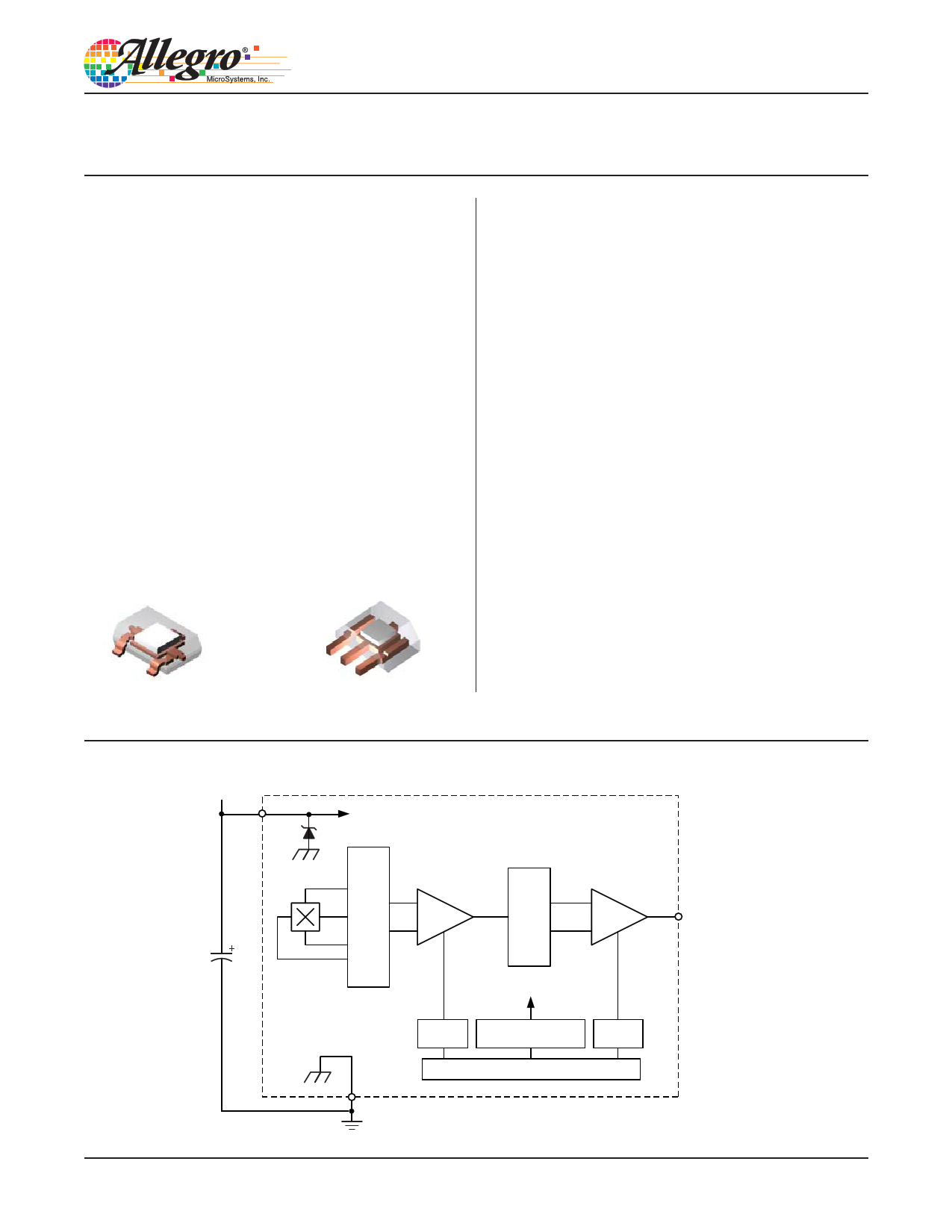
Not to scale
V+
VCC
Continued on the next page…
Functional Block Diagram
To all subcircuits
CBYPASS
A1381-DS, Rev. 1
Amp
VOUT
Out (Programming)
GND
Hall Drive Circuit
Gain
Gain Temperature
Coefficient
Offset
Trim Control
1 page 
A1381, A1382,
A1383, and A1384
Programmable Linear Hall Effect Sensors with Analog Output
Available in a Miniature Thin Profile Surface Mount Package
OPERATING CHARACTERISTICS (continued), valid over full operating temperature range,TA; CBYPASS= 0.1 μF, VCC = 5 V, unless otherwise specified
Characteristic
Symbol
Test Conditions
Min. Typ. Max. Units
ERROR COMPONENTS
Linearity Sensitivity Error
Symmetry Sensitivity Error
Ratiometry Quiescent Voltage
Output Error13
LinERR
SymERR
RatERRVOUT(Q)
– ±1.5
– ±1.5
– ±1.5
–%
–%
–%
Ratiometry Sensitivity Error13
Ratiometry Clamp Error14
DRIFT CHARACTERISTICS
RatERRSens
RatERRCLP
TA = 25°C
– ±1.5
– ±1.5
–%
–%
A1381
– – ±60 mV
Quiescent Voltage Output Drift
Through Temperature Range
∆VOUT(Q)
A1382
A1383 TA = 150°C
– – ±50 mV
– – ±40 mV
A1384
– – ±40 mV
Sensitivity Drift Through
Temperature Range15
∆SensTC
– ±3 – %
Sensitivity Drift Due to Package
Hysteresis1
∆SensPKG TA = 25°C; after temperature cycling
– ±2 – %
1See Characteristic Definitions section.
2fC varies up to approximately ± 20% over the full operating ambient temperature range, TA, and process.
3Unit of measure (phase degrees) in reference to the magnetic input signal.
4Sens, VOUT(Q), VCLP(LOW) , and VCLP(HIGH) scale with VCC due to ratiometry.
5Raw device characteristic values before any programming.
6Programmed at 150°C and calculated relative to 25°C.
7VOUT(Q)(max) is the value available with all programming fuses blown (maximum programming code set). The VOUT(Q) range is the total range from
VOUT(Q)init up to and including VOUT(Q)(max). See Characteristic Definitions section.
8Step size is larger than required, in order to provide for manufacturing spread. See Characteristic Definitions section.
9Non-ideal behavior in the programming DAC can cause the step size at each significant bit rollover code to be greater than twice the maximum
specified value of StepVOUT(Q) , StepSENS , or StepTCSENS.
10Overall programming value accuracy. See Characteristic Definitions section.
11Sens(max) is the value available with all programming fuses blown (maximum programming code set). Sens range is the total range from Sensinit up
to and including Sens(max). See Characteristic Definitions section.
12Default polarity is for VOUT voltage to increase with a positive (south polarity) field applied to the branded face of the device.
13Percent change from actual value at VCC = 5 V, for a given temperature, over the guaranteed supply voltage operating range.
14Percent change from actual value at VCC = 5 V, TA = 25°C, over the guaranteed supply voltage operating range.
15Sensitivity drift from expected value at TA after programming TCSENS. See Characteristic Definitions section.
Allegro MicroSystems, Inc.
5
115 Northeast Cutoff, Box 15036
Worcester, Massachusetts 01615-0036 (508) 853-5000
www.allegromicro.com
5 Page 
A1381, A1382,
A1383, and A1384
Programmable Linear Hall Effect Sensors with Analog Output
Available in a Miniature Thin Profile Surface Mount Package
Programming Guidelines
Overview
Definition of Terms
Programming is accomplished by sending a series of input volt-
age pulses serially through the VOUT pin of the device. A unique
combination of different voltage level pulses controls the internal
programming logic of the device to select a desired program-
mable parameter and change its value. There are two program-
ming pulses, referred to as a high voltage pulse, VPH, consisting
of a VP(LOW) –VP(HIGH) –VP(LOW) sequence and a mid voltage
pulse, VPM, consisting of a VP(LOW) –VP(MID) –VP(LOW) sequence.
The 138x features Try mode, Blow mode, and Lock mode:
Register. The section of the programming logic that controls the
choice of programmable modes and parameters.
Bit Field. The internal fuses unique to each register, represented
as a binary number. Incrementing the bit field of a particular
register causes its programmable parameter to change, based on
the internal programming logic.
Key. A series of VPM voltage pulses used to select a register, with
a value expressed as the decimal equivalent of the binary value.
The LSB of a register is denoted as key 1, or bit 0.
• In Try mode, the value of a single programmable parameter may
be set and measured. The parameter value is stored temporar-
ily, and resets after cycling the supply voltage. Note that other
parameters cannot be accessed simultaneously in this mode.
• In Blow mode, the value of a single programmable parameter
may be permanently set by blowing solid-state fuses internal to
the device. Additional parameters may be blown sequentially.
• In Lock mode, a device-level fuse is blown, blocking the fur-
ther programming of all parameters.
The programming sequence is designed to help prevent the
device from being programmed accidentally; for example, as a
result of noise on the supply line.
Although any programmable variable power supply can be used
to generate the pulse waveforms, Allegro highly recommends
using the Allegro Sensor Evaluation Kit, available on the Allegro
Web site On-line Store. The manual for that kit is available for
download free of charge, and provides additional information on
programming these devices.
Code. The number used to identify the combination of fuses
activated in a bit field, expressed as the decimal equivalent of the
binary value. The LSB of a bit field is denoted as code 1, or bit 0.
Addressing. Incrementing the bit field code of a selected register
by serially applying a pulse train through the VOUT pin of the
device. Each parameter can be measured during the addressing
process, but the internal fuses must be blown before the program-
ming code (and parameter value) becomes permanent.
Fuse Blowing. Applying a VPH voltage pulse of sufficient dura-
tion at the VP(HIGH) level to permanently set an addressed bit by
blowing a fuse internal to the device. Once a bit (fuse) has been
blown, it cannot be reset.
Blow Pulse. A VPH voltage pulse of sufficient duration at the
VP(HIGH) level to blow the addressed fuse.
Cycling the Supply. Powering-down, and then powering-up the
supply voltage. Cycling the supply is used to clear the program-
ming settings in Try mode.
Programming Pulse Requirements, Protocol at TA = 25°C
Characteristic Symbol
Notes
Programming Voltage
Programming Current
VP(LOW)
VP(MID)
VP(HIGH)
IP
Measured at the VOUT pin.
Minimum supply current required to ensure proper fuse blowing. In addition, a min-
imum capacitance, CBLOW = 0.1 μF, must be connected between the VOUT and
GND pins during programming to provide the current necessary for fuse blowing.
Pulse Width
Pulse Rise Time
Pulse Fall Time
tOFF(HIGH)
tOFF(MID)
tACTIVE(HIGH)
tACTIVE(MID)
tBLOW
tPr
tPf
Duration at VP(LOW) level following a VP(HIGH) level.
Duration at VP(LOW) level following a VP(MID) level.
Duration of VP(HIGH) level for VPH pulses during key/code selection.
Duration of VP(MID) level for VPH pulses during key/code selection.
Duration at VP(HIGH) level for fuse blowing.
Rise time required for transitions from VP(LOW) to either VP(MID) or VP(HIGH).
Fall time required for transitions from VP(HIGH) to either VP(MID) to VP(LOW).
Min.
-
14
26
300
30
5
30
15
30
1
1
Typ. Max. Units
- 5.5 V
15 16 V
27 28 V
- - mA
- - μs
- - μs
- - μs
- - μs
- - μs
- 100 μs
- 100 μs
Allegro MicroSystems, Inc.
11
115 Northeast Cutoff, Box 15036
Worcester, Massachusetts 01615-0036 (508) 853-5000
www.allegromicro.com
11 Page | ||
| Páginas | Total 18 Páginas | |
| PDF Descargar | [ Datasheet A1381.PDF ] | |
Hoja de datos destacado
| Número de pieza | Descripción | Fabricantes |
| A1380 | PNP Transistor - 2SA1380 | Sanyo |
| A1381 | (A1381 - A1384) Programmable Linear Hall Effect Sensors | Allegro MicroSystems |
| A1382 | (A1381 - A1384) Programmable Linear Hall Effect Sensors | Allegro MicroSystems |
| A1383 | (A1381 - A1384) Programmable Linear Hall Effect Sensors | Allegro MicroSystems |
| Número de pieza | Descripción | Fabricantes |
| SLA6805M | High Voltage 3 phase Motor Driver IC. |
Sanken |
| SDC1742 | 12- and 14-Bit Hybrid Synchro / Resolver-to-Digital Converters. |
Analog Devices |
|
DataSheet.es es una pagina web que funciona como un repositorio de manuales o hoja de datos de muchos de los productos más populares, |
| DataSheet.es | 2020 | Privacy Policy | Contacto | Buscar |