|
|
|
PDF VSC838 Data sheet ( Hoja de datos )
| Número de pieza | VSC838 | |
| Descripción | 3.2Gb/s 36x37 Crosspoint Switch | |
| Fabricantes | Vitesse Semiconductor | |
| Logotipo | ||
Hay una vista previa y un enlace de descarga de VSC838 (archivo pdf) en la parte inferior de esta página. Total 20 Páginas | ||
|
No Preview Available !
www.DataSheet4U.com
VITESSE
SEMICONDUCTOR CORPORATION
Preliminary Data Sheet
VSC838
3.2Gb/s
36x37 Crosspoint Switch
Features
• 36 Input by 37 Output Crosspoint Switch
• 3.2Gb/s NRZ Data Bandwidth
• Non-Blocking Architecture Broadcast and Multicast
Capabilities
• LVTTL/2.5V CMOS Control I/O (3.3V tolerant)
• Input Signal Activity Monitoring Function
• Integrated Signal Equalization (ISE) for Deterministic
Jitter Reduction
• 66MHz Dual Programming Port
• Parallel and Serial programming modes
• Programmable On-Chip I/O Termination
• Differential CML Output Drivers
• Single 2.5V Supply
• 6W Typical—Low Drive Mode
7W Typical—High Drive Mode
• High Performance 37.5mm, 480 TBGA Package
General Description
The VSC838 is a monolithic 36x36 asynchronous crosspoint switch, designed to carry broadband data
streams. The VSC838 also has an internal 37th output channel which is used in conjunction with the Activity
Monitor to allow in system diagnostics.
A high degree of signal integrity is maintained throughout the chip via fully differential signal paths.
The crosspoint function is based on a multiplexer array architecture. Each data output is driven by a 36:1
multiplexer that can be programmed to one and only one of its 36 inputs. The signal path is unregistered and
fully asynchronous, so there are not any restrictions on the phase, frequency, or signal pattern at each input.
Each high-speed output is a fully differential, switched current driver with switchable on-die terminations
for maximum signal integrity. Data inputs are terminated on-die through 100Ω impedance between true and
complement inputs (see Input Termination section for further details).
A dual mode programming interface is provided that allows programming commands to be sent as serial
data or parallel data. Core programming can be random for each port address, or multiple program assignments
can be queued and issued simultaneously. The programming may be initialized to a “straight-through” configu-
ration (A0 to Y0, A1 to Y1, etc.) using the INIT pin.
Unused channels may be powered down to allow efficient use of the switch in applications that require only
a subset of the channels. Power-down can be accomplished in hardware, via dedicated power pins for pairs of
input and output channels, or in software by programming individual unused outputs with a disable code.
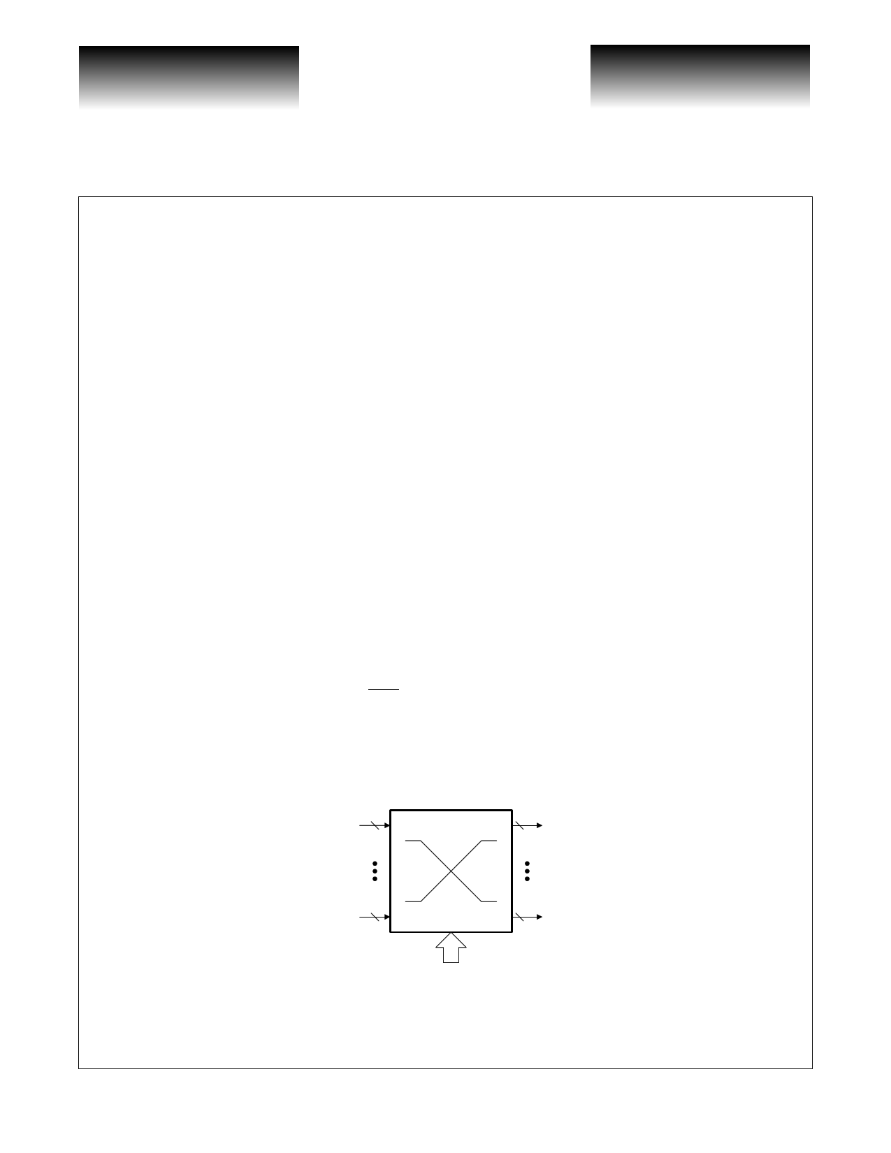
VSC838 Block Diagram
A0 2
2 Y0
A35 2
µP
control
2 Y35
G52351-0, Rev 3.0
02/12/01
© VITESSE SEMICONDUCTOR CORPORATION • 741 Calle Plano • Camarillo, CA 93012
Tel: (800) VITESSE • FAX: (805) 987-5896 • Email: [email protected]
Internet: www.vitesse.com
Page 1
1 page 
VITESSE
SEMICONDUCTOR CORPORATION
Preliminary Data Sheet
VSC838
3.2Gb/s
36x37 Crosspoint Switch
AC Characteristics
Table 1: Data Path
Parameter
Description
Min Typ Max Units
fRATE
TSKW
TPDAY
tR, tF
tR, tF
tjR
tjP
NOTES:
Maximum data rate
- - 3.2 Gb/s
Channel-to-channel delay skew
- 300 -
ps
Propagation Delay from an A input to a Y output
- 750 -
ps
High-speed input rise/fall times, 20% to 80%
- - 150 ps
High-speed output rise/fall times, 20% to 80%
Output added delay jitter, rms(1, 2)
Output added delay jitter, peak-to-peak(1, 2)
- - 150 ps
- 10 ps
- 40 ps
(1) Tested on a sample basis only. (2) Broadband (unfiltered) deterministic jitter added to a jitter-free input, 223-1 PRBS data pattern.
Table 2: Program Interface Timing
Parameter
Description
Min Typ Max Units
TsWR
Setup time from INCHAN[5:0] or OUTCHAN5:0] to rising edge of
WR.
3.35 —
—
ThWR
Hold time from rising edge of WRB to INCHAN[5:0] or
OUTCHAN[5:0].
1.45 —
—
TPWLW
TsCS
Pulse width (HIGH or LOW) on LOAD
Setup time from CS to falling edge of LOAD or ALE_SCN in parallel or
burst mode, or rising edge of LOAD in serial mode.
6.75
0
—
—
—
—
ThCSB
Hold time of CS rising edge after LOAD or ALE_SCN rising in parallel
or burst mode, or falling edge of LOAD in serial mode, or falling edge of
CONFIG in any mode.
0
——
TPWCFG
TsSDIN
ThSDIN
TperSCLK
TsLOAD
ThLOAD
TsSERIAL
Pulse width (HIGH or LOW) on CONFIG.
Setup time from INCHAN0(SDIN) to INCHAN1(SCLK) rising.
Hold time of INCHAN0(SDIN) after INCHAN1(SCLK) rising.
Minimum period of SCLK in serial mode.
Setup time from LOAD to INCHAN1(SCLK) rising.
Hold time of LOAD after INCHAN1(SCLK) rising.
Setup time from SERIAL rising to INCHAN1(SCLK) rising when
entering serial mode or SERIAL falling to LOAD falling when entering
parallel mode or SERIAL falling to LOAD rising when entering burst
mode.
6.75
1.65
1.0
15
1.85
0.95
0.90
—
—
—
—
—
—
—
—
—
—
—
—
—
—
ThSERIAL
Hold time from INCHAN1(SCLK) rising to SERIAL falling when
exiting serial mode.
0 ——
TdSDOUT
TPWINIT
TsSCAN
Delay from INCHAN1(SCLK) rising to SDOUT, 20pF load.
— — 6.20
Pulse width (HIGH or LOW) on INIT.
6.75 —
—
Setup time from ALE_SCN to INCHAN1(SCLK) rising when starting
or completing a serial read-back sequence.
1.65
—
—
ThSCAN
Hold time of ALE_SCN after INCHAN1(SCLK) rising when starting or
completing a serial read-back sequence.
1.0
—
—
ns
ns
ns
ns
ns
ns
ns
ns
ns
ns
ns
ns
ns
ns
ns
ns
ns
G52351-0, Rev 3.0
02/12/01
© VITESSE SEMICONDUCTOR CORPORATION • 741 Calle Plano • Camarillo, CA 93012
Internet: www.vitesse.com
Page 5
5 Page 
VITESSE
SEMICONDUCTOR CORPORATION
Preliminary Data Sheet
VSC838
3.2Gb/s
36x37 Crosspoint Switch
Figure 5: Pinout Diagram -- Bottom View
29 28 27 26 25 24 23 22 21 20 19 18 17 16 15 14 13 12 11 10 9
8
7
6
5
4
3
2
1
Ball grid
index
NC NC NC NC NC NC NC NC NC OUTCHAN4
AA
NC 2 NC 6 NC 10 NC 14 NC 18 NC 22 NC 26 NC 30 NC 34 OUTCHAN5
BB
NC NC NC NC NC NC NC NC NC NC
CC
NC NC NC NC NC NC NC NC NC NC
DD
NC 0 NC 4 NC 8 NC 12 NC 16 NC 20 NC 24 NC 28 NC 32 NC
EE
FF
G Inputs [An, ANn]
H
G
H
JJ
KK
LL
M
N VCC
M
N
P Dedicated VEE
P
RR
T
Common VEE (always On)
T
U Control port
V
U
V
WW
YY
AA AA
AB AB
AC Inputs [An, ANn]
AD
NC NC NC NC NC NC NC NC SERIAL
AE
INCHAN1(SCLK) 3 NC 7 NC 11 NC 15 NC 19 NC 23 NC 27 NC 31 NC 35 CS
AF
AG
INCHAN0(SDIN)
NC
NC
NC
NC
NC
NC
NC
NC SDOUT
INCHAN2
NC
NC
NC
NC
NC
NC
NC
NC
AH
INCHAN3 1 NC 5 NC 9 NC 13 NC 17 NC 21 NC 25 NC 29 NC 33 INIT
AJ
AC
AD
AE
AF
AG
AH
AJ
29 28 27 26 25 24 23 22 21 20 19 18 17 16 15 14 13 12 11 10 9 8 7 6 5 4 3 2 1
G52351-0, Rev 3.0
02/12/01
© VITESSE SEMICONDUCTOR CORPORATION • 741 Calle Plano • Camarillo, CA 93012
Internet: www.vitesse.com
Page 11
11 Page | ||
| Páginas | Total 20 Páginas | |
| PDF Descargar | [ Datasheet VSC838.PDF ] | |
Hoja de datos destacado
| Número de pieza | Descripción | Fabricantes |
| VSC830 | 2.7Gb/s Asynchronous Dual 2x2 Crosspoint Switch | Vitesse Semiconductor |
| VSC834 | 2.5Gb/s 17 x 17 Crosspoint Switch | Vitesse Semiconductor |
| VSC835 | 34x34 Crosspoint Switch | Vitesse Semiconductor |
| VSC837 | 3.2Gb/s 68x68 Crosspoint Switch | Vitesse Semiconductor |
| Número de pieza | Descripción | Fabricantes |
| SLA6805M | High Voltage 3 phase Motor Driver IC. |
Sanken |
| SDC1742 | 12- and 14-Bit Hybrid Synchro / Resolver-to-Digital Converters. |
Analog Devices |
|
DataSheet.es es una pagina web que funciona como un repositorio de manuales o hoja de datos de muchos de los productos más populares, |
| DataSheet.es | 2020 | Privacy Policy | Contacto | Buscar |