|
|
PDF TC1017 Data sheet ( Hoja de datos )
| Número de pieza | TC1017 | |
| Descripción | Tiny CMOS LDO | |
| Fabricantes | Microchip Technology | |
| Logotipo |  |
|
Hay una vista previa y un enlace de descarga de TC1017 (archivo pdf) en la parte inferior de esta página. Total 22 Páginas | ||
|
No Preview Available !
www.DataSheet4U.com
M
TC1017
150 mA, Tiny CMOS LDO With Shutdown
Features
• Space-saving 5-Pin SC-70 and SOT-23
Packages
• Extremely Low Operating Current for Longer
Battery Life: 53 µA (typ.)
• Very Low Dropout Voltage
• Rated 150 mA Output Current
• Requires Only 1 µF Ceramic Output Capacitance
• High Output Voltage Accuracy: ±0.5% (typ.)
• 10 µsec (typ.) Wake-Up Time from SHDN
• Power-Saving Shutdown Mode: 0.05 µA (typ.)
• Overcurrent and Overtemperature Protection
• Pin Compatible Upgrade for Bipolar Regulators
Applications
• Cellular/GSM/PHS Phones
• Battery Operated Systems
• Portable Computers
• Medical Instruments
• Electronic Games
• Pagers
General Description
The TC1017 is a high-accuracy (typically ±0.5%)
CMOS upgrade for bipolar low dropout regulators. It is
offered in a SC-70 or SOT-23 package. The SC-70
package represents a 50% reduced footprint versus
the popular SOT-23 package.
Developed specifically for battery-powered systems,
the TC1017’s CMOS construction consumes only
53 µA typical supply current over the entire 150 mA
operating load range. This can be as much as 60 times
less than the quiescent operating current consumed by
bipolar LDOs.
With small-space requirements and cost in mind, the
TC1017 was developed to be stable over the entire
input voltage and output current operating range using
low value (1 µF ceramic), low equivalent series
resistance output capacitors. Additional integrated
features, such as shutdown, overcurrent and
overtemperature protection, further reduce the board
space and cost of the entire voltage regulating
application.
Key performance parameters for the TC1017 are low
dropout voltage (285 mV typical at 150 mA output
current), low supply current while shutdown (0.05 µA
typical) and fast stable response to sudden input
voltage and load changes.
Package Types
SC-70
VIN
5
VOUT
4
TC1017
SOT-23
12 3
SHDN NC GND
VOUT
NC
54
TC1017
12 3
VIN GND SHDN
2003 Microchip Technology Inc.
DS21813B-page 1
1 page 
TC1017
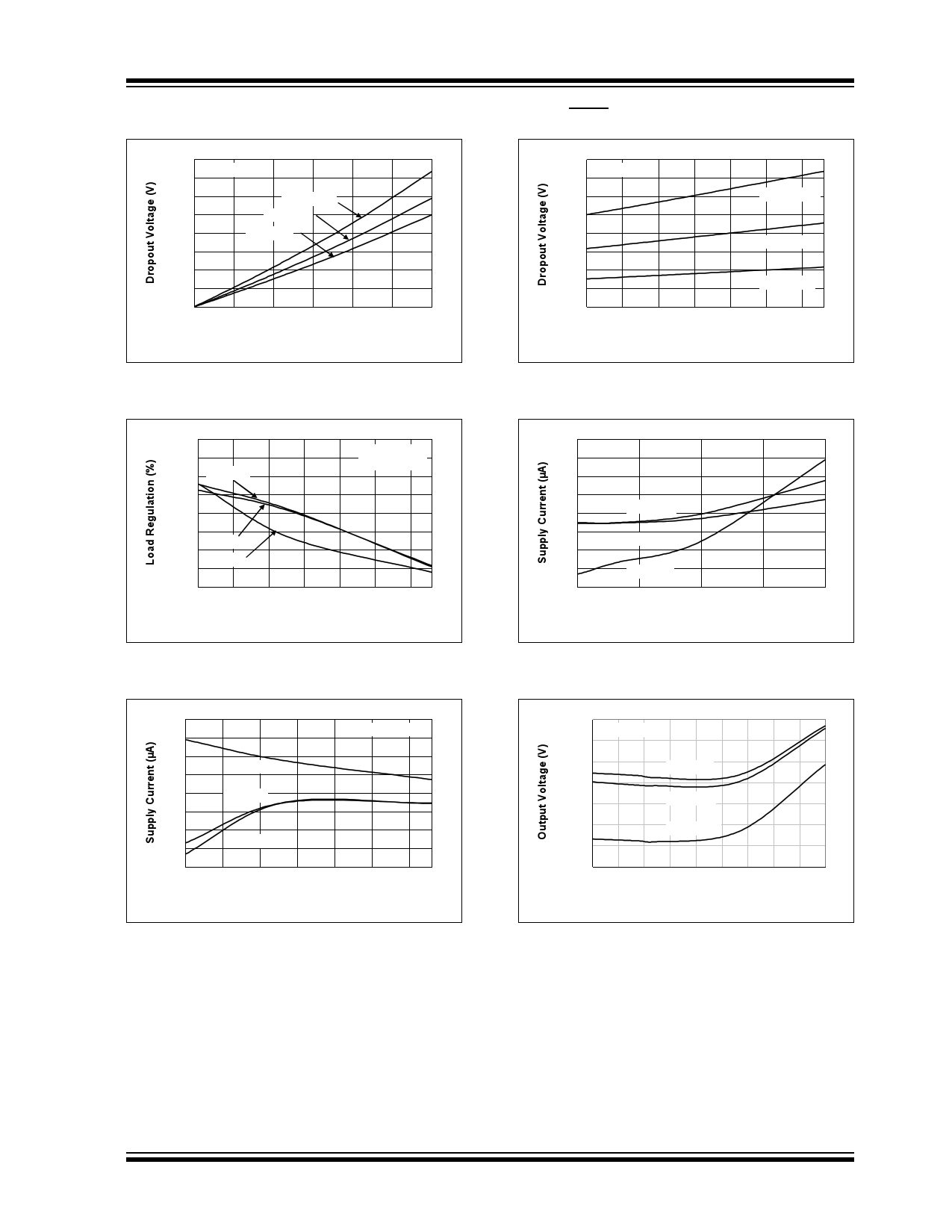
Note: Unless otherwise noted, VIN = VR + 1V, IL = 100 µA, CL = 1.0 µF, SHDN > VIH, TA = +25°C.
0.40
0.35
VOUT = 3.30V
0.30
0.25
TA = +125°C
TA = +25°C
0.20
TA = -40°C
0.15
0.10
0.05
0.00
0
25 50 75 100 125 150
Load Current (mA)
FIGURE 2-7:
Current.
Dropout Voltage vs. Output
0.40
0.35
0.30
VOUT = 3.30V
IOUT = 150 mA
0.25
0.20
0.15
IOUT = 100 mA
0.10
0.05
IOUT = 50 mA
0.00
-40 -15 10 35 60 85 110
Temperature (°C)
FIGURE 2-10:
Temperature.
Dropout Voltage vs.
-0.30
-0.35
-0.40
VIN = 6.0V
-0.45
-0.50
-0.55
-0.60
-0.65
VIN = 4.3V
VIN = 4.0V
-0.70
-40
-15
VOUT = 3.30V
IOUT = 0-150 mA
10 35 60 85
Temperature (°C)
110
FIGURE 2-8:
Temperature.
Load Regulation vs.
60
59 VOUT = 3.30V
58
57
56 TA = +25°C
55 TA = +125°C
54
53
52
4.0
TA = -40°C
4.5
5.0
5.5
Input Voltage (V)
6.0
FIGURE 2-11:
Voltage.
Supply Current vs. Input
60
59
58
57
56
55
54
53
52
-40
VIN = 6.0V
VIN = 4.3V
VOUT = 3.30V
VIN = 4.0V
-15 10 35 60 85 110
Temperature (°C)
FIGURE 2-9:
Temperature.
Supply Current vs.
2.869
2.868
VOUT = 2.85V
2.867
2.866
2.865
TA = -40°C
TA = +25°C
2.864
2.863
TA = +125°C
2.862
3.3 3.6 3.9 4.2 4.5 4.8 5.1 5.4 5.7 6.0
Input Voltage (V)
FIGURE 2-12:
Voltage.
Output Voltage vs. Supply
2003 Microchip Technology Inc.
DS21813B-page 5
5 Page 
4.1 Input Capacitor
Low input source impedance is necessary for the LDO
to operate properly. When operating from batteries, or
in applications with long lead length (> 10") between
the input source and the LDO, some input capacitance
is required. A minimum of 0.1 µF is recommended for
most applications and the capacitor should be placed
as close to the input of the LDO as is practical. Larger
input capacitors will help reduce the input impedance
and further reduce any high-frequency noise on the
input and output of the LDO.
4.2 Output Capacitor
A minimum output capacitance of 1 µF for the TC1017
is required for stability. The equivalent series resis-
tance (ESR) requirements on the output capacitor are
between 0 and 2 ohms. The output capacitor should be
located as close to the LDO output as is practical.
Ceramic materials X7R and X5R have low temperature
coefficients and are well within the acceptable ESR
range required. A typical 1 µF X5R 0805 capacitor has
an ESR of 50 milli-ohms. Larger output capacitors can
be used with the TC1017 to improve dynamic behavior
and input ripple-rejection performance.
Ceramic, aluminum electrolytic or tantalum capacitor
types can be used. Since many aluminum electrolytic
capacitors freeze at approximately –30°C, ceramic or
solid tantalums are recommended for applications
operating below –25°C. When operating from sources
other than batteries, supply-noise rejection and
transient response can be improved by increasing the
value of the input and output capacitors and employing
passive filtering techniques.
TC1017
4.3 Turn-On Response
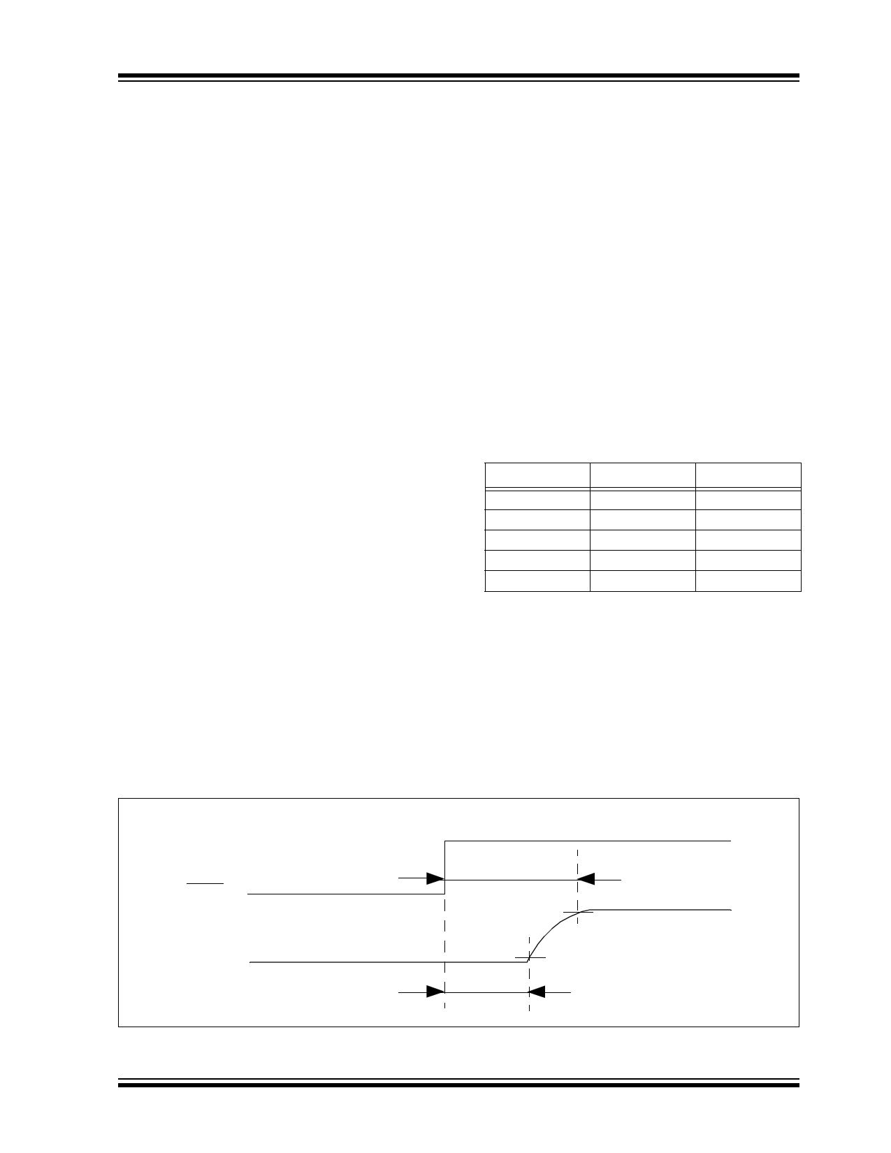
The turn-on response is defined as two separate
response categories, wake-up time (tWK) and settling
time (tS).
The TC1017 has a fast wake-up time (10 µsec, typical)
when released from shutdown. See Figure 4-3 for the
wake-up time designated as tWK. The wake-up time is
defined as the time it takes for the output to rise to 2%
of the VOUT value after being released from shutdown.
The total turn-on response is defined as the settling
time (tS) (see Figure 4-3). Settling time (inclusive with
tWK) is defined as the condition when the output is
within 98% of its fully-enabled value (32 µsec, typical)
when released from shutdown. The settling time of the
output voltage is dependent on load conditions and
output capacitance on VOUT (RC response).
The table below demonstrates the typical turn-on
response timing for different input voltage power-up
frequencies: VOUT = 2.85V, VIN = 5.0V, IOUT = 60 mA
and COUT = 1 µF.
Frequency
1000 Hz
500 Hz
100 Hz
50 Hz
10 Hz
Typical (tWK)
5.3 µsec
5.9 µsec
9.8 µsec
14.5 µsec
17.2 µsec
Typical (tS)
14 µsec
16 µsec
32 µsec
52 µsec
77 µsec
SHDN
VOUT
VIL
FIGURE 4-3:
Wake-Up Time from Shutdown.
2003 Microchip Technology Inc.
VIH
tS
98%
2%
tWK
DS21813B-page 11
11 Page | ||
| Páginas | Total 22 Páginas | |
| PDF Descargar | [ Datasheet TC1017.PDF ] | |
Hoja de datos destacado
| Número de pieza | Descripción | Fabricantes |
| TC1014 | CMOS LDOs | Microchip Technology |
| TC1014 | 50mA CMOS LDO WITH SHUTDOWN AND REFERENCE BYPASS | TelCom Semiconductor |
| TC1015 | CMOS LDOs | Microchip Technology |
| TC1016 | 80MA TINY CMOS LDO WITH SHUTDOWN | Microchip Technology |
| Número de pieza | Descripción | Fabricantes |
| SLA6805M | High Voltage 3 phase Motor Driver IC. |
Sanken |
| SDC1742 | 12- and 14-Bit Hybrid Synchro / Resolver-to-Digital Converters. |
Analog Devices |
|
DataSheet.es es una pagina web que funciona como un repositorio de manuales o hoja de datos de muchos de los productos más populares, |
| DataSheet.es | 2020 | Privacy Policy | Contacto | Buscar |
