|
|
|
PDF INA-32063 Data sheet ( Hoja de datos )
| Número de pieza | INA-32063 | |
| Descripción | Wideband Silicon RFIC Amplifier | |
| Fabricantes | Hewlett-Packard | |
| Logotipo | ||
Hay una vista previa y un enlace de descarga de INA-32063 (archivo pdf) en la parte inferior de esta página. Total 11 Páginas | ||
|
No Preview Available !
www.DataSheet4U.com
3.0 GHz Wideband Silicon
RFIC Amplifier
Technical Data
INA-32063
Features
• 17 dB Gain at 1.9 GHz
• +3 dBm P1 dB at 1.9 GHz
• Single +3V Supply
• Unconditionally Stable
Applications
• LO Buffer and Driver
Amplifier for Cellular,
Cordless, Special Mobile
Radio, PCS, ISM, Wireless
LAN, DBS, TVRO, and TV
Tuner
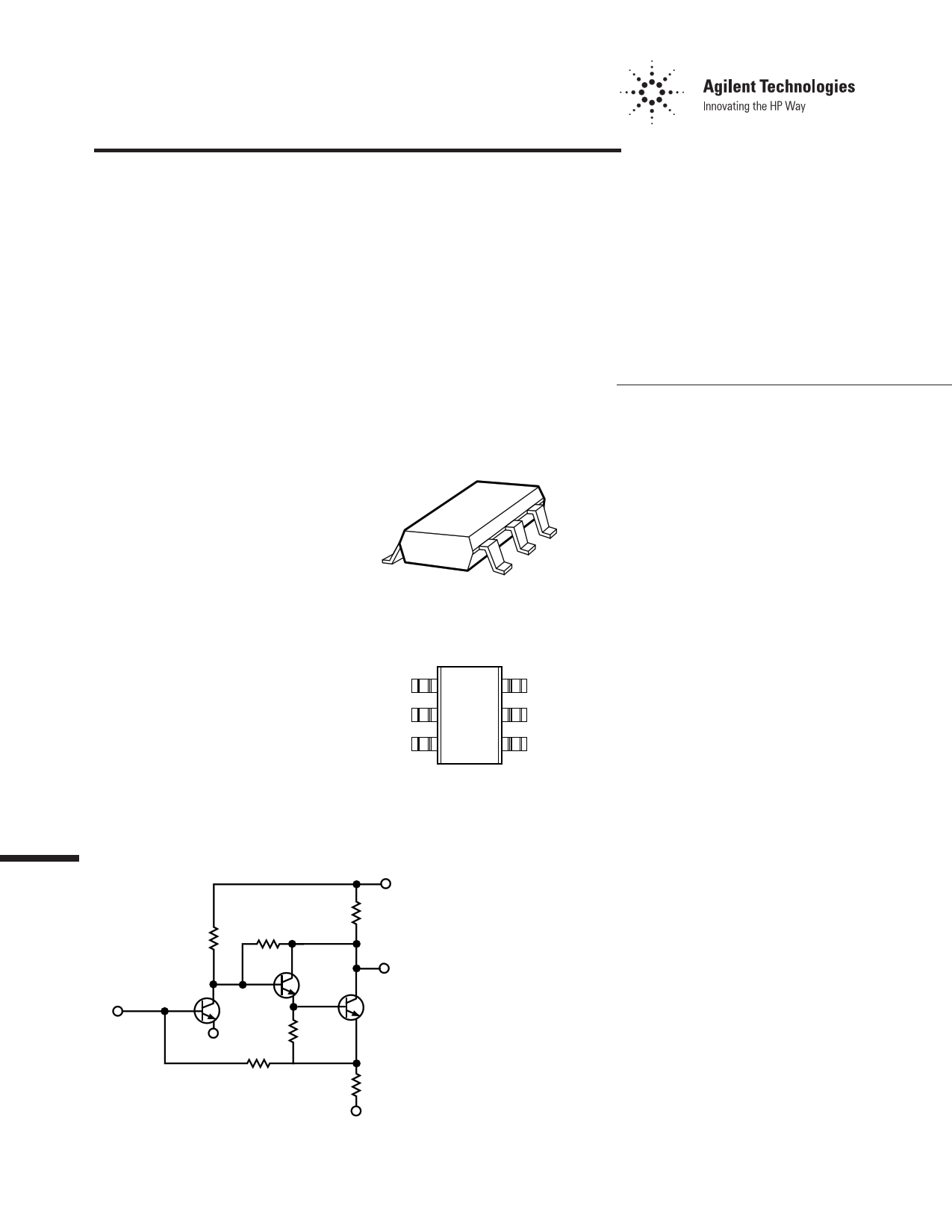
Simplified Schematic
Surface Mount SOT-363
(SC-70) Package
Pin Connections and
Package Marking
GND 2 1
GND 1 2
INPUT 3
6 OUTPUT
& Vd
5 GND 1
4 Vd
Note: Package marking provides
orientation and identification.
Vd
Output & Vd
Description
Agilent’s INA-32063 is a Silicon
RFIC amplifier that offers
excellent gain and output power
for applications to 3.0 GHz.
Packaged in an ultraminiature
SOT-363 package, it requires half
of the board space of a SOT-143
package.
The INA-32063 offers wide
bandwidth and good linearity and
17 dB gain with a modest supply
current. With its input and output
matched internally to 50 Ω, the
INA-32063 is a simple to use gain
block that is suitable for
numerous applications.
The INA-32063 is fabricated using
Agilent’s 30 GHz – fmax,
ISOSAT™ Silicon-bipolar process
that uses nitride, self-alignment,
submicrometer lithography,
trench isolation, ion implantation,
and polyimide intermetal dielec-
tric and scratch protection to
achieve superior performance,
uniformity and reliability.
Input
Gnd1
Gnd2
1 page 
5
INA-32063 Applications
Information
Introduction
The INA-32063 is a +3 volt silicon
RFIC amplifier that is designed
with a two stage internal network
to provide a broadband gain and
50 Ω input and output impedance.
With a typical +4.8 dBm P-1 dB
compressed output power at
1900 MHz, for only 20 mA supply
current. The broad bandwidth,
INA-32063, is well suited for
amplifier applications in mobile
communication systems.
A feature of the INA-32063 is a
positive gain slope over the
1–2.5 GHz range that is useful in
many satellite-based TV and
datacom systems.
In addition to use in buffer and
driver amplifier applications in
the cellular market, the
INA-32063 will find many
applications in battery operated
wireless communication systems.
Operating Details
The INA-32063 is a voltage-biased
device that operates from a
+3 volt power supply with a
typical current drain of 20 mA. All
bias regulation circuitry is
integrated into the RFIC.
Figure 10 shows a typical imple-
mentation of the INA-32063. The
supply voltage for the INA-32063
must be applied to two terminals,
the Vd pin and the RF Output pin.
Gnd2
Gnd1
Gnd1
Cout
RF
Output
RFC
RF
Input
Cblock
Vd
Cbypass
Figure 10. Basic Amplifier
Application.
The Vd connection to the ampli-
fier is RF bypassed by placing a
capacitor to ground near the Vd
pin of the amplifier package.
The power supply connection to
the RF Output pin is achieved by
means of a RF choke (inductor).
The value of the RF choke must
be large relative to 50 Ω in order
to prevent loading of the RF
Output. The supply voltage end of
the RF choke is bypassed to
ground with a capacitor. If the
physical layout permits, this can
be the same bypass capacitor that
is used at the Vd terminal of the
amplifier.
Blocking capacitors are normally
placed in series with the RF Input
and the RF Output to isolate the
DC voltages on these pins from
circuits adjacent to the amplifier.
The values for the blocking and
bypass capacitors are selected to
provide a reactance at the lowest
frequency of operation that is
small relative to 50 Ω.
Example Layout for 50 Ω
Output Amplifier
An example layout for an ampli-
fier using the INA-32063 with
50 Ω input and 50 Ω output is
shown in Figure 11.
Gnd 1
RF Input
50 Ω
Gnd 2
50 Ω
Gnd 1
RF Output
and Vd
Figure 11. RF Layout.
This example uses a
microstripline design (solid
groundplane on the backside of
the circuit board). The circuit
board material is 0.031-inch thick
FR-4. Plated through holes (vias)
are used to bring the ground to
the topside of the circuit where
needed. The performance of
INA-32063 is sensitive to ground
path inductance. The two-stage
design creates the possibility of a
feedback loop being formed
through the ground returns of the
stages, Gnd 1 and Gnd 2.
Gnd 1
Gnd 2
VIA
Figure 12. INA-32063 Potential
Ground Loop.
Gnd 1
VIA
Gnd 2
VIA
Figure 13. INA-32063 Suggested
Layout.
At least one ground via should be
placed adjacent to each ground
pin to assure good RF grounding.
Multiple vias are used to reduce
the inductance of the path to
ground and should be placed as
close to the package terminals as
practical.
The effects of the potential
ground loop shown in Figure 12
may be observed as a “peaking” in
the gain versus frequency
response, an increase in input
VSWR, or even as return gain at
the input of the INA-32063.
Figure 14 shows an assembled
amplifier. The +3 volt supply is
fed directly into the Vd pin of the
5 Page 
www.semiconductor.agilent.com
Data subject to change.
Copyright © 1999 Agilent Technologies
Obsoletes 5965-8921E
5967-5769E (11/99)
11 Page | ||
| Páginas | Total 11 Páginas | |
| PDF Descargar | [ Datasheet INA-32063.PDF ] | |
Hoja de datos destacado
| Número de pieza | Descripción | Fabricantes |
| INA-32063 | Wideband Silicon RFIC Amplifier | Hewlett-Packard |
| Número de pieza | Descripción | Fabricantes |
| SLA6805M | High Voltage 3 phase Motor Driver IC. |
Sanken |
| SDC1742 | 12- and 14-Bit Hybrid Synchro / Resolver-to-Digital Converters. |
Analog Devices |
|
DataSheet.es es una pagina web que funciona como un repositorio de manuales o hoja de datos de muchos de los productos más populares, |
| DataSheet.es | 2020 | Privacy Policy | Contacto | Buscar |