|
|
|
PDF AD9627 Data sheet ( Hoja de datos )
| Número de pieza | AD9627 | |
| Descripción | Dual Analog-to-Digital Converter | |
| Fabricantes | Analog Devices | |
| Logotipo | ||
Hay una vista previa y un enlace de descarga de AD9627 (archivo pdf) en la parte inferior de esta página. Total 30 Páginas | ||
|
No Preview Available !
12-Bit, 80 MSPS/105 MSPS/125 MSPS/150 MSPS,
1.8 V Dual Analog-to-Digital Converter
AD9627
FEATURES
SNR = 69.4 dBc (70.4 dBFS) to 70 MHz @ 125 MSPS
SFDR = 85 dBc to 70 MHz @ 125 MSPS
Low power: 750 mW @ 125 MSPS
SNR = 69.2 dBc (70.2 dBFS) to 70 MHz @ 150 MSPS
SFDR = 84 dBc to 70 MHz @ 150 MSPS
Low power: 820 mW @ 150 MSPS
1.8 V analog supply operation
1.8 V to 3.3 V CMOS output supply or 1.8 V LVDS
output supply
Integer 1-to-8 input clock divider
IF sampling frequencies to 450 MHz
Internal ADC voltage reference
Integrated ADC sample-and-hold inputs
Flexible analog input range: 1 V p-p to 2 V p-p
Differential analog inputs with 650 MHz bandwidth
ADC clock duty cycle stabilizer
95 dB channel isolation/crosstalk
Serial port control
User-configurable, built-in self-test (BIST) capability
Energy-saving power-down modes
Integrated receive features
Fast detect/threshold bits
Composite signal monitor
APPLICATIONS
Communications
Diversity radio systems
Multimode digital receivers (3G)
GSM, EDGE, WCDMA,
CDMA2000, WiMAX, TD-SCDMA
I/Q demodulation systems
Smart antenna systems
General-purpose software radios
Broadband data applications
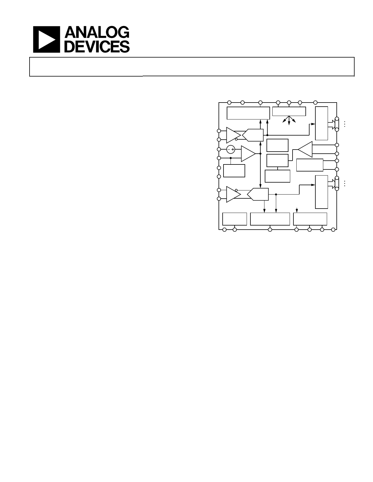
FUNCTIONAL BLOCK DIAGRAM
SDIO/ SCLK/
AVDD DVDD FD(0:3)A DCS DFS CSB DRVDD
FD BITS/THRESHOLD
DETECT
SPI
VIN+A
VIN–A
VREF
SENSE
CML
RBIAS
VIN–B
VIN+B
SHA
REF
SELECT
ADC
PROGRAMMING DATA
SIGNAL
MONITOR
DIVIDE
1 TO 8
DUTY CYCLE
STABILIZER
DCO
GENERATION
SHA
AD9627
ADC
SIGNAL MONITOR
DATA
MULTICHIP FD BITS/THRESHOLD SIGNAL MONITOR
SYNC
DETECT
INTERFACE
D11A
D0A
CLK+
CLK–
DCOA
DCOB
D11B
D0B
AGND SYNC
FD(0:3)B
SMI SMI SMI DRGND
SDFS SCLK/ SDO/
PDWN OEB
NOTES
1. PIN NAMES ARE FOR THE CMOS PIN CONFIGURATION ONLY;
SEE FIGURE 7 FOR LVDS PIN NAMES.
Figure 1.
PRODUCT HIGHLIGHTS
1. Integrated dual, 12-bit, 80 MSPS/105 MSPS/125 MSPS/
150 MSPS ADC.
2. Fast overrange detect and signal monitor with serial output.
3. Signal monitor block with dedicated serial output mode.
4. Proprietary differential input that maintains excellent SNR
performance for input frequencies up to 450 MHz.
5. Operation from a single 1.8 V supply and a separate digital
output driver supply to accommodate 1.8 V to 3.3 V logic
families.
6. Standard serial port interface (SPI) that supports various
product features and functions, such as data formatting
(offset binary, twos complement, or gray coding), enabling
the clock DCS, power-down, test modes, and voltage
reference mode.
7. Pin compatibility with the AD9640, AD9627-11, and AD9600
for a simple migration from 12 bits to 14 bits, 11 bits, or
10 bits.
Rev. B
Information furnished by Analog Devices is believed to be accurate and reliable. However, no
responsibility is assumed by Analog Devices for its use, nor for any infringements of patents or other
rights of third parties that may result from its use. Specifications subject to change without notice. No
license is granted by implication or otherwise under any patent or patent rights of Analog Devices.
Trademarksandregisteredtrademarksarethepropertyoftheirrespectiveowners.
One Technology Way, P.O. Box 9106, Norwood, MA 02062-9106, U.S.A.
Tel: 781.329.4700
www.analog.com
Fax: 781.461.3113 ©2007–2010 Analog Devices, Inc. All rights reserved.
1 page 
AD9627
GENERAL DESCRIPTION
The AD9627 is a dual, 12-bit, 80 MSPS/105 MSPS/125 MSPS/
150 MSPS analog-to-digital converter (ADC). The AD9627 is
designed to support communications applications where low
cost, small size, and versatility are desired.
The dual ADC core features a multistage, differential pipelined
architecture with integrated output error correction logic. Each
ADC features wide bandwidth differential sample-and-hold
analog input amplifiers supporting a variety of user-selectable
input ranges. An integrated voltage reference eases design consid-
erations. A duty cycle stabilizer is provided to compensate for
variations in the ADC clock duty cycle, allowing the converters
to maintain excellent performance.
The AD9627 has several functions that simplify the automatic
gain control (AGC) function in the system receiver. The fast detect
feature allows fast overrange detection by outputting four bits of
input level information with very short latency.
In addition, the programmable threshold detector allows moni-
toring of the incoming signal power, using the four fast detect
bits of the ADC with very low latency. If the input signal level
exceeds the programmable threshold, the coarse upper threshold
indicator goes high. Because this threshold indicator has very
low latency, the user can quickly turn down the system gain to
avoid an overrange condition.
The second AGC-related function is the signal monitor. This block
allows the user to monitor the composite magnitude of the
incoming signal, which aids in setting the gain to optimize the
dynamic range of the overall system.
The ADC output data can be routed directly to the two external
12-bit output ports. These outputs can be set from 1.8 V to 3.3 V
CMOS or 1.8 V LVDS.
Flexible power-down options allow significant power savings,
when desired.
Programming for setup and control is accomplished using a 3-bit
SPI-compatible serial interface.
The AD9627 is available in a 64-lead LFCSP and is specified over
the industrial temperature range of −40°C to +85°C.
Rev. B | Page 4 of 76
5 Page 
AD9627
Parameter
Input Resistance
Input Capacitance
DIGITAL OUTPUTS
CMOS Mode—DRVDD = 3.3 V
High Level Output Voltage
IOH = 50 μA
IOH = 0.5 mA
Low Level Output Voltage
IOL = 1.6 mA
IOL = 50 μA
CMOS Mode—DRVDD = 1.8 V
High Level Output Voltage
IOH = 50 μA
IOH = 0.5 mA
Low Level Output Voltage
IOL = 1.6 mA
IOL = 50 μA
LVDS Mode—DRVDD = 1.8 V
Differential Output Voltage (VOD), ANSI Mode
Output Offset Voltage (VOS), ANSI Mode
Differential Output Voltage (VOD), Reduced Swing Mode
Output Offset Voltage (VOS), Reduced Swing Mode
1 Pull up.
2 Pull down.
Temperature
Full
Full
Min
Full 3.29
Full 3.25
Full
Full
Full 1.79
Full 1.75
Full
Full
Full 250
Full 1.15
Full 150
Full 1.15
Typ Max
26
5
Unit
kΩ
pF
0.2
0.05
0.2
0.05
350 450
1.25 1.35
200 280
1.25 1.35
V
V
V
V
V
V
V
V
mV
V
mV
V
Rev. B | Page 10 of 76
11 Page | ||
| Páginas | Total 30 Páginas | |
| PDF Descargar | [ Datasheet AD9627.PDF ] | |
Hoja de datos destacado
| Número de pieza | Descripción | Fabricantes |
| AD9620 | Ultralow Distortion Buffer | Analog Devices |
| AD9621 | Wideband Voltage Feedback Amplifier | Analog Devices |
| AD9622 | Wideband Voltage Feedback Amplifier | Analog Devices |
| AD9623 | Wideband Voltage Feedback Amplifier | Analog Devices |
| Número de pieza | Descripción | Fabricantes |
| SLA6805M | High Voltage 3 phase Motor Driver IC. |
Sanken |
| SDC1742 | 12- and 14-Bit Hybrid Synchro / Resolver-to-Digital Converters. |
Analog Devices |
|
DataSheet.es es una pagina web que funciona como un repositorio de manuales o hoja de datos de muchos de los productos más populares, |
| DataSheet.es | 2020 | Privacy Policy | Contacto | Buscar |