|
|
PDF AD8190 Data sheet ( Hoja de datos )
| Número de pieza | AD8190 | |
| Descripción | 2:1 HDMI/DVI Switch | |
| Fabricantes | Analog Devices | |
| Logotipo |  |
|
Hay una vista previa y un enlace de descarga de AD8190 (archivo pdf) en la parte inferior de esta página. Total 24 Páginas | ||
|
No Preview Available !
www.DataSheet4U.com
2:1 HDMI/DVI Switch with Equalization
AD8190
FEATURES
Two inputs, one output HDMI/DVI links
Enables HDMI 1.2a-compliant receiver
Four TMDS channels per link
Supports 250 Mbps to 1.65 Gbps data rates
Supports 25 MHz to 165 MHz pixel clocks
Equalized inputs for operation with long HDMI cables
(20 meters at 1080p)
Fully buffered unidirectional inputs/outputs
Globally switchable 50 Ω on-chip terminations
Pre-emphasized outputs
Low added jitter
Single-supply operation (3.3 V)
Four auxiliary channels per link
Bidirectional unbuffered inputs/outputs
Flexible supply operation (3.3 V to 5 V)
HDCP standard compatible
Allows switching of DDC bus and two additional signals
Output disable feature
Reduced power dissipation
Output termination removal
Two AD8190s support HDMI/DVI dual-link
Standards compliant: HDMI receiver, HDCP, DVI
Serial (I2C slave) control interface
56-lead, 8 mm x 8 mm, LFCSP, Pb-free package
APPLICATIONS
Multiple input displays
Projectors
A/V receivers
Set-top boxes
Advanced television (HDTV) sets
GENERAL DESCRIPTION
The AD8190 is an HDMI/DVI switch featuring equalized
TMDS inputs and pre-emphasized TMDS outputs, ideal for
systems with long cable runs. Outputs can be set to a high
impedance state to reduce the power dissipation and/or allow
the construction of larger arrays using the wire-OR technique.
The AD8190 is provided in a space saving, 56-lead, LFCSP,
surface-mount, Pb-free, plastic package and is specified to
operate over the −40°C to +85°C temperature range.
FUNCTIONAL BLOCK DIAGRAM
I2C_SDA
I2C_SCL
I2C_ADDR
VTTI
RESET
SERIAL INTERFACE
CONFIG
INTERFACE
CONTROL
LOGIC
AD8190
AVCC
DVCC
AMUXVCC
AVEE
DVEE
IP_A[3:0]
IN_A[3:0]
+
–
IP_B[3:0]
IN_B[3:0]
+
–
4
4
SWITCH
4
CORE
4 EQ
PE 4
4
HIGH SPEED
BUFFERED
VTTO
+
OP[3:0]
ON[3:0]
–
VTTI
AUX_A[3:0]
AUX_B[3:0]
4
4
SWITCH
CORE
4
LOW SPEED UNBUFFERED
BIDIRECTIONAL
AUX_COM[3:0]
Figure 1.
SET-TOP BOX
TYPICAL APPLICATION
HDTV SET
HDMI
RECEIVER
DVD PLAYER
AD8190
DVD
01:18
Figure 2. Typical AD8190 Application for HDTV Sets
PRODUCT HIGHLIGHTS
1. Supports data rates up to 1.65 Gbps, enabling UXGA
(1600 × 1200) DVI resolutions and 1080p HDMI formats.
2. Input cable equalizer enables use of long cables at the
input (more than 20 meters of 24 AWG cable at 1080p).
3. Auxiliary switch allows routing of the DDC bus and two
additional single-ended signals for a single chip, fully
HDMI 1.2a receive-compliant solution.
Rev. 0
Information furnished by Analog Devices is believed to be accurate and reliable. However, no
responsibility is assumed by Analog Devices for its use, nor for any infringements of patents or other
rights of third parties that may result from its use. Specifications subject to change without notice. No
license is granted by implication or otherwise under any patent or patent rights of Analog Devices.
Trademarksandregisteredtrademarksarethepropertyoftheirrespectiveowners.
One Technology Way, P.O. Box 9106, Norwood, MA 02062-9106, U.S.A.
Tel: 781.329.4700
www.analog.com
Fax: 781.461.3113
©2006 Analog Devices, Inc. All rights reserved.
1 page 
ABSOLUTE MAXIMUM RATINGS
Table 2.
Parameter
Rating
AVCC to AVEE
DVCC to DVEE
3.7 V
3.7 V
DVEE to AVEE
±0.3 V
VTTI AVCC + 0.6 V
VTTO
AVCC + 0.6 V
AMUXVCC
Internal Power Dissipation
High Speed Input Voltage
High Speed Differential
Input Voltage
Low Speed Input Voltage
I2C Logic Input Voltage
Storage Temperature
Range
5.5 V
4.62 W
AVCC − 1.4 V < VIN < AVCC + 0.6 V
2.0 V
DVEE − 0.3 V < VIN < AMUXVCC + 0.6 V
DVEE − 0.3 V < VIN < DVCC + 0.6 V
−65°C to +125°C
Operating Temperature
Range
−40°C to +85°C
Junction Temperature
150°C
Stresses above those listed under Absolute Maximum Ratings
may cause permanent damage to the device. This is a stress
rating only; functional operation of the device at these or any
other conditions above those indicated in the operational
section of this specification is not implied. Exposure to absolute
maximum rating conditions for extended periods may affect
device reliability.
AD8190
THERMAL RESISTANCE
θJA is specified for the worst-case conditions: a device soldered
in a 4-layer JEDEC circuit board for surface-mount packages.
θJC is specified for the exposed pad soldered to the circuit board
with no airflow.
Table 3. Thermal Resistance
Package Type
θJA
56-Lead LFCSP
27
θJC Unit
2.1 °C/W
MAXIMUM POWER DISSIPATION
The maximum power that can be safely dissipated by the
AD8190 is limited by the associated rise in junction tempera-
ture. The maximum safe junction temperature for plastic
encapsulated devices is determined by the glass transition
temperature of the plastic, approximately 150°C. Temporarily
exceeding this limit may cause a shift in parametric performance
due to a change in the stresses exerted on the die by the package.
Exceeding a junction temperature of 175°C for an extended
period can result in device failure. To ensure proper operation,
it is necessary to observe the maximum power derating as
determined by the coefficients in Table 3.
ESD CAUTION
ESD (electrostatic discharge) sensitive device. Electrostatic charges as high as 4000 V readily accumulate on
the human body and test equipment and can discharge without detection. Although this product features
proprietary ESD protection circuitry, permanent damage may occur on devices subjected to high energy
electrostatic discharges. Therefore, proper ESD precautions are recommended to avoid performance
degradation or loss of functionality.
Rev. 0 | Page 5 of 24
5 Page 
AD8190
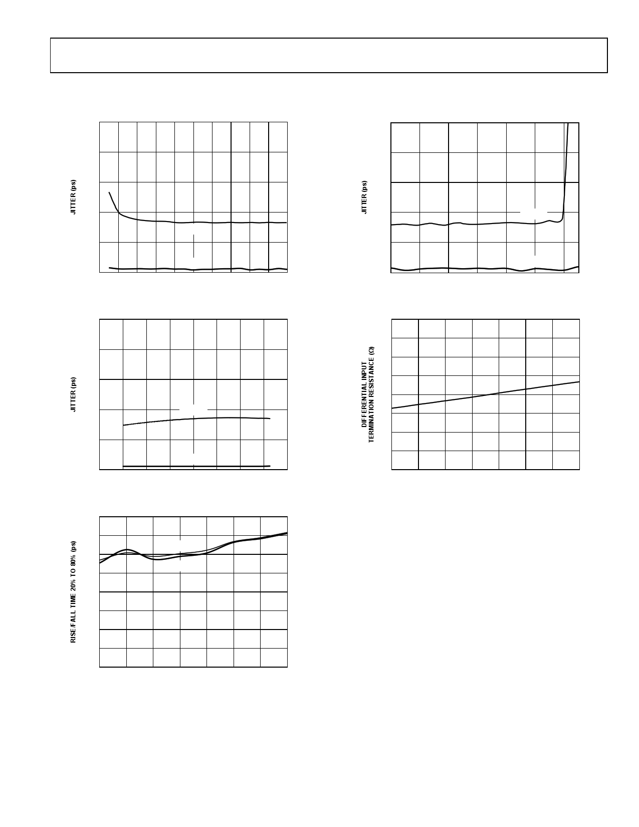
TA = 27°C, AVCC = 3.3 V, VTTI = 3.3 V, VTTO = 3.3 V, DVCC = 3.3 V, AMUXVCC = 5 V, AVEE = 0 V, DVEE = 0 V, differential input swing =
1000 mV, TMDS outputs terminated with external 50 Ω resistors to 3.3 V, pattern = PRBS 27 − 1, data rate = 1.65 Gbps, unless otherwise noted.
50 50
40 40
30 30
20
DJ (p-p)
10
RJ (rms)
0
0 0.2 0.4 0.6 0.8 1.0 1.2 1.4 1.6 1.8 2.0
DIFFERENTIAL INPUT SWING (V)
Figure 20. Jitter vs. Differential Input Swing
50
40
30
20 DJ (p-p)
10
0
–60
160
RJ (rms)
–40 –20
0
20 40 60
TEMPERATURE (°C)
Figure 21. Jitter vs. Temperature
80
140
FALL TIME
120
RISE TIME
100
80
60
40
20
0
–40 –20
0
20 40 60 80
TEMPERATURE (°C)
Figure 22. Rise and Fall Time vs. Temperature
100
100
20 DJ (p-p)
10
RJ (rms)
0
2.5 2.7 2.9 3.1 3.3 3.5 3.7
INPUT COMMON-MODE VOLTAGE (V)
Figure 23. Jitter vs. Input Common-Mode Voltage
120
115
110
105
100
95
90
85
80
–40
–20
0
20 40 60 80 100
TEMPERATURE (°C)
Figure 24. Differential Input Termination Resistance vs. Temperature
Rev. 0 | Page 11 of 24
11 Page | ||
| Páginas | Total 24 Páginas | |
| PDF Descargar | [ Datasheet AD8190.PDF ] | |
Hoja de datos destacado
| Número de pieza | Descripción | Fabricantes |
| AD8190 | 2:1 HDMI/DVI Switch | Analog Devices |
| AD8191 | HDMI/DVI Switch | Analog Devices |
| AD8192 | 2:1 HDMI/DVI Switch | Analog Devices |
| AD8193 | Buffered 2:1 TMDS Switch | Analog Devices |
| Número de pieza | Descripción | Fabricantes |
| SLA6805M | High Voltage 3 phase Motor Driver IC. |
Sanken |
| SDC1742 | 12- and 14-Bit Hybrid Synchro / Resolver-to-Digital Converters. |
Analog Devices |
|
DataSheet.es es una pagina web que funciona como un repositorio de manuales o hoja de datos de muchos de los productos más populares, |
| DataSheet.es | 2020 | Privacy Policy | Contacto | Buscar |
