|
|
|
PDF AD8134 Data sheet ( Hoja de datos )
| Número de pieza | AD8134 | |
| Descripción | Triple Differential Driver | |
| Fabricantes | Analog Devices | |
| Logotipo | ||
Hay una vista previa y un enlace de descarga de AD8134 (archivo pdf) en la parte inferior de esta página. Total 21 Páginas | ||
|
No Preview Available !
Data Sheet
FEATURES
Triple high speed differential driver
225 MHz, −3 dB large signal bandwidth
450 MHz, −3 dB small signal bandwidth
Easily drives 1.4 V p-p video signal into doubly terminated
100 Ω UTP cable
1600 V/µs slew rate
Fixed internal gain of 2
Internal common-mode feedback network
Output balance error −60 dB @ 50 MHz
On-chip sync-on-common-mode circuitry
Output pull-down feature for line isolation
Differential input and output
Differential-to-differential or single-ended-to-differential
operation
High isolation between amplifiers: 80 dB @ 10 MHz
Low distortion: 64 dB SFDR @ 10 MHz on 5 V supply,
RL, dm = 200 Ω
Low offset: 3 mV typical output-referred on 5 V supply
Low power: 26.5 mA @ 5 V for three drivers and sync circuitry
Wide supply voltage range: +5 V to ±5 V
Available in space-saving packaging: 4 mm × 4 mm LFCSP
APPLICATIONS
Keyboard-video-mouse (KVM) networking
GENERAL DESCRIPTION
The AD8134 is a major advancement beyond using discrete
op amps for driving differential RGB signals over twisted pair
cable. The AD8134 is a triple, low cost differential or single-
ended input to differential output driver, and each amplifier has
a fixed gain of 2 to compensate for the attenuation of the line
termination resistors. The AD8134 is specifically designed for
RGB signals but can be used for any type of analog signals or
high speed data transmission. The AD8134 is capable of driving
either Category 5 (Cat-5) unshielded twisted pair (UTP) cable
or differential printed circuit board transmission lines with
minimal signal degradation.
A unique feature that allows the user to transmit balanced
horizontal and vertical video sync signals over the three
common-mode channels with minimal electromagnetic
interference (EMI) radiation is included on-chip.
The outputs of the AD8134 can be set to a low voltage state that
allows easy differential multiplexing of multiple drivers on the
same twisted pair cable, when used with external series diodes.
Triple Differential Driver
With Sync-On-Common-Mode
AD8134
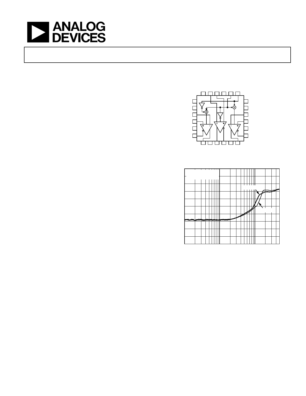
FUNCTIONAL BLOCK DIAGRAM
24 23 22 21 20 19
AD8134
OPD 1
VS– 2
–IN R 3
×2
+IN R 4
G
VS– 5
R
B
–OUT R 6
18 SYNC LEVEL
17 VS+ (SYNC)
16 –IN B
15 +IN B
14 VS–
13 –OUT B
7 8 9 10 11 12
Figure 1.
0
∆VOUT, dm = 2V p-p
–10 ∆VOUT, cm/∆VOUT, dm
–20
–30
VS = ±5V
–40
–50
VS = +5V
–60
–70
–80
–90
–100
1
10 100
FREQUENCY (MHz)
Figure 2. Output Balance vs. Frequency
500
The AD8134 driver is a natural complement to the AD8143,
AD8129, and AD8130 differential receivers.
Manufactured on the Analog Devices next generation XFCB
bipolar process, the AD8134 has a large signal bandwidth of
225 MHz and a slew rate of 1600 V/µs. The AD8134 has an
internal common-mode feedback feature that provides output
gain and phase matching that is balanced to −60 dB at 50 MHz,
suppressing harmonics and reducing radiated EMI.
The AD8134 is available in a 24-lead LFCSP and can operate
over the −40°C to +85°C extended industrial temperature range.
Rev. B
Document Feedback
Information furnished by Analog Devices is believed to be accurate and reliable. However, no
responsibilityisassumedbyAnalogDevices for itsuse,nor foranyinfringementsofpatentsor other
rights of third parties that may result from its use. Specifications subject to change without notice. No
license is granted by implication or otherwise under any patent or patent rights of Analog Devices.
Trademarksandregisteredtrademarksarethepropertyoftheirrespectiveowners.
One Technology Way, P.O. Box 9106, Norwood, MA 02062-9106, U.S.A.
Tel: 781.329.4700 ©2004–2016 Analog Devices, Inc. All rights reserved.
Technical Support
www.analog.com
1 page 
AD8134
Data Sheet
VS+ = 5 V, VS− = 0 V, HSYNC and VSYNC = VS−, RL, dm = 200 Ω @ 25°C, unless otherwise noted. TMIN to TMAX = −40°C to +85°C.
Table 2.
Parameter
DIFFERENTIAL INPUT PERFORMANCE
DYNAMIC PERFORMANCE
−3 dB Small Signal Bandwidth
−3 dB Large Signal Bandwidth
Bandwidth for 0.1 dB Flatness
Slew Rate
Settling Time to 0.1%
Isolation Between Amplifiers
DIFFERENTIAL INPUT CHARACTERISTICS
Input Common-Mode Voltage Range
Input Resistance
Input Capacitance
DC CMRR
DIFFERENTIAL OUTPUT CHARACTERISTICS
Differential Signal Gain
Output Voltage Swing
Output Offset Voltage
Output Offset Drift
Output Balance Error
Output Voltage Noise
Output Short-Circuit Current
COMMON-MODE SYNC PERFORMANCE
SYNC DYNAMIC PERFORMANCE
Slew Rate
HSYNC AND VSYNC INPUTS
Input Low Voltage
Input High Voltage
SYNC LEVEL INPUT
Input Voltage Range
Setting to Achieve 0.5 V Pulse Levels
Gain to Red Common-Mode Output
Gain to Green Common-Mode Output
Gain to Blue Common-Mode Output
POWER SUPPLY
Operating Range
Quiescent Current
PSRR
OUTPUT PULL-DOWN PERFORMANCE
OPD Input Low Voltage
OPD Input High Voltage
OPD Input Bias Current
OPD Assert Time
OPD De-Assert Time
Output Voltage When OPD Asserted
Conditions
VO = 0.2 V p-p
VO = 2 V p-p
VO = 0.2 V p-p
VO = 2 V p-p, 25% to 75%
VO = 2 V step
f = 10 MHz, between Amplifier R and
Amplifier G
Differential
Single-ended input
Differential
ΔVOUT, dm/ΔVIN, cm, ΔVIN, cm = ±1 V
ΔVOUT, dm/ΔVIN, dm, ΔVIN, dm = ±1 V
Each single-ended output
TMIN to TMAX
f = 50 MHz
DC
f = 1 MHz
VOUT, cm = −1 V to +1 V; 25% to 75%
For linear operation
ΔVO, cm/ΔVSYNC LEVEL
ΔVO, cm/ΔVSYNC LEVEL
ΔVO, cm/ΔVSYNC LEVEL
Each output, OPD input @ VS+
Min Typ
Max
400
200
50
1400
14
75
0 to 5
1.5
1.13
1
−48
1.920
VS− + 1.25
−24
1.955
3
±30
−60
−70
25
90
2.000
VS+ − 1.15
+24
−54
700
VS− to 1.10
1.40 to VS+
VS− + 0.5
0.97 1.02
1.94 2.03
0.96 1.02
1.06
2.10
1.05
+4.5
26.5
−54
±6
27.5
−48
VS− to VS+ − 3.85
VS+ − 2.85 to VS+
63
100
100
VS− + 0.79
80
VS− + 0.82
Unit
MHz
MHz
MHz
V/µs
ns
dB
V
kΩ
kΩ
pF
dB
V/V
V
mV
µV/°C
dB
dB
nV/√Hz
mA
V/µs
V
V
V
V
V/V
V/V
V/V
V
mA
dB
V
V
µA
ns
ns
V
Rev. B | Page 4 of 20
5 Page 
AD8134
2
1
0
–1
–2
–3
–4
–5
1000
RL, dm = ∞
SINGLE-ENDED OUTPUT
OUTPUT
PULL-DOWN
VOUTN
100ns/DIV VON
Figure 18. Output Pull-Down Response
100
10
10 100 1k
10k 100k 1M 10M 100M
FREQUENCY (Hz)
Figure 19. Output-Referred Voltage Noise vs. Frequency
0
∆VOUT, dm = 2V p-p
–10 ∆VOUT, cm/∆VOUT, dm
–20
–30
VS = ±5V
–40
–50
VS = +5V
–60
–70
–80
–90
–100
1
10 100
FREQUENCY (MHz)
Figure 20. Output Balance vs. Frequency
500
Data Sheet
–30
∆VOUT, dm/∆VIN, cm
–35 ∆VIN, cm = 200mV p-p
–40
–45
VS = +5V
VS = ±5V
–50
–55
–60
–65
1
10 100
FREQUENCY (MHz)
Figure 21. Common-Mode Rejection Ratio vs. Frequency
10
∆VOUT, dm/∆VS
0
1000
–10
–20
–30
–40 PSRR+
–50
PSRR–
–60
–70
0.1
1 10 100
FREQUENCY (MHz)
Figure 22. Power Supply Rejection Ratio vs. Frequency
1000
–40
RED TO GREEN
VIN, dm = 200mV p-p
–50 ∆VOUT, dm G/∆VIN, dm R
–60
–70 VIN, dm = 2V p-p
–80
–90
–100
–110
1
10 100
FREQUENCY (MHz)
Figure 23. Amplifier-to-Amplifier Isolation vs. Frequency
1000
Rev. B | Page 10 of 20
11 Page | ||
| Páginas | Total 21 Páginas | |
| PDF Descargar | [ Datasheet AD8134.PDF ] | |
Hoja de datos destacado
| Número de pieza | Descripción | Fabricantes |
| AD813 | Low Power Triple Video Amplifier | Analog Devices |
| AD8130 | (AD8129 / AD8130) Low Cost 270 MHz Differential Receiver Amplifiers | Analog Devices |
| AD8131 | Low-Cost / High-Speed Differential Driver | Analog Devices |
| AD8132 | Low-Cost/ High-Speed Differential Amplifier | Analog Devices |
| Número de pieza | Descripción | Fabricantes |
| SLA6805M | High Voltage 3 phase Motor Driver IC. |
Sanken |
| SDC1742 | 12- and 14-Bit Hybrid Synchro / Resolver-to-Digital Converters. |
Analog Devices |
|
DataSheet.es es una pagina web que funciona como un repositorio de manuales o hoja de datos de muchos de los productos más populares, |
| DataSheet.es | 2020 | Privacy Policy | Contacto | Buscar |