|
|
|
PDF AD8128 Data sheet ( Hoja de datos )
| Número de pieza | AD8128 | |
| Descripción | CAT-5 Receiver | |
| Fabricantes | Analog Devices | |
| Logotipo | ||
1. AD8128 Hay una vista previa y un enlace de descarga de AD8128 (archivo pdf) en la parte inferior de esta página. Total 13 Páginas | ||
|
No Preview Available !
Data Sheet
CAT-5 Receiver with
Adjustable Line Equalization
AD8128
FEATURES
Tuned to compensate for Category-5 (CAT-5) cable losses
Up to 100 meters at 120 MHz
2 voltage controlled frequency response adjustment pins
High frequency peaking adjustment
Broadband gain adjustment
2700 V/μs slew rate
Low output noise
1.5 mV rms integrated noise (1 GHz) at 100 meters
equalized bandwidth
DC output offset adjust
Low offset voltage error: 7 mV typ
Equalized pass-band ripple ±1 dB to 70 MHz
Input: differential or single ended
Supply current: 24 mA on ±5 V
Small 8-lead 3 mm × 3 mm LFCSP
APPLICATIONS
Keyboard-video-mouse (KVM)
RGB video over unshielded twisted pair (UTP) cable receivers
Professional video projection and distribution
Security video
GENERAL DESCRIPTION
The AD8128 is a high speed, differential receiver/equalizer that
compensates for the transmission losses of unshielded twisted pair
(UTP) CAT-5 cables. Various frequency dependent gain stages
are summed together to best approximate the inverse frequency
response of CAT-5/CAT-5e cable. An equalized bandwidth of
120 MHz can be achieved for 100 meters of cable.
The AD8128 can be used as a standalone receiver/equalizer or
in conjunction with the AD8143, triple differential receiver, to
provide a complete low cost solution for receiving RGB over
UTP cable in such applications as KVM.
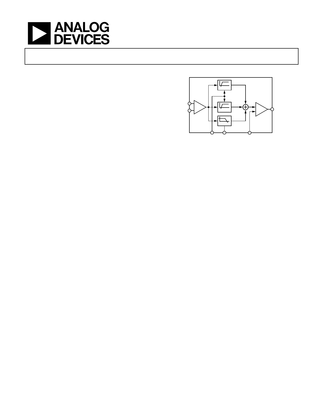
FUNCTIONAL BLOCK DIAGRAM
AD8128
HPF
VIN+
VIN–
HPF
LPF
VPEAK VGAIN
VOFFSET
Figure 1.
VOUT
The AD8128 has three control pins for optimal CAT-5/CAT-5e
compensation. The equalized cable length is directly proportional
to the voltage applied to the VPEAKpin, which controls the amount
of high frequency peaking. VGAIN adjusts the broadband gain
from 0 dB to 3 dB, compensating for the resistive cable loss.
VOFFSET allows the output to be shifted by ±2.5 V, adding
flexibility for dc-coupled systems.
Low integrated output noise and offset voltage adjust make the
AD8128 an excellent choice for dc-coupled wideband RGB-over-
CAT-5 applications. For systems where the UTP cable is longer
than 100 meters, two AD8128 devices can be cascaded to
compensate for up to 200 meters of CAT-5/CAT-5e.
The AD8128 is available in a 3 mm × 3 mm 8-lead LFCSP and
is rated to operate over the extended temperature range of
−40°C to +85°C.
Rev. A
Document Feedback
Information furnished by Analog Devices is believed to be accurate and reliable. However, no
responsibility is assumed by Analog Devices for its use, nor for any infringements of patents or other
rights of third parties that may result from its use. Specifications subject to change without notice. No
license is granted by implication or otherwise under any patent or patent rights of Analog Devices.
Trademarksandregisteredtrademarksarethepropertyoftheirrespectiveowners.
One Technology Way, P.O. Box 9106, Norwood, MA 02062-9106, U.S.A.
Tel: 781.329.4700 ©2005–2016 Analog Devices, Inc. All rights reserved.
Technical Support
www.analog.com
1 page 
AD8128
ABSOLUTE MAXIMUM RATINGS
Table 2.
Parameter
Supply Voltage
Input Voltage
VPEAK and VGAIN Control Pins
VOFFSET Control Pins
Operating Temperature Range
Storage Temperature Range
Lead Temperature (Soldering 10 sec)
Junction Temperature
Rating
±5.5 V
±VS
−3 V to +VS
±VS
−40°C to +85°C
−65°C to +125°C
300°C
150°C
Stresses at or above those listed under Absolute Maximum
Ratings may cause permanent damage to the product. This is a
stress rating only; functional operation of the product at these
or any other conditions above those indicated in the operational
section of this specification is not implied. Operation beyond
the maximum operating conditions for extended periods may
affect product reliability.
THERMAL RESISTANCE
θJA is specified for the worst-case conditions, that is, a device
soldered in a circuit board for surface-mount packages.
Table 3. Thermal Resistance
Package Type
θJA θJC Unit
8-Lead LFCSP
77 14 °C/W
Maximum Power Dissipation
The maximum safe power dissipation in the AD8128 package is
limited by the associated rise in junction temperature (TJ) on the
die. At approximately 150°C, which is the glass transition temp-
erature, the plastic changes the properties. Even temporarily
exceeding this temperature limit can change the stresses that the
package exerts on the die, permanently shifting the parametric
performance of the AD8128. Exceeding a junction temperature
of 150°C for an extended period can result in changes in the
silicon devices potentially causing failure.
Data Sheet
The power dissipated in the package (PD) is the sum of the
quiescent power dissipation and the power dissipated in the
package due to the load drive for the output. The quiescent power
is the voltage between the supply pins (VS) times the quiescent
current (IS). The power dissipated due to the load drive depends
upon the particular application. For each output, the power due
to load drive is calculated by multiplying the load current by the
associated voltage drop across the
Airflow increases heat dissipation, effectively reducing θJA. Also,
more metal directly in contact with the package leads from metal
traces, through-holes, ground, and power planes reduces the θJA.
The exposed pad on the underside of the package must be
soldered to a pad on the PCB surface, which is thermally connected
to a copper plane to achieve the specified θJA.
Figure 2 shows the maximum safe power dissipation in the package
vs. the ambient temperature for the 8-lead LFCSP (48.5°C/W) on a
JEDEC standard 4-layer board with the underside pad soldered to a
pad that is thermally connected to a PCB plane. Extra thermal
relief is required for operation at high supply voltages.
3.0
2.5
2.0
1.5
1.0
0.5
0
–40 –30 –20 –10 0 10 20 30 40 50 60 70 80 90 100 110 120 130
AMBIENT TEMPERATURE (°C)
Figure 2. Maximum Power Dissipation vs. Temperature
ESD CAUTION
Rev. A | Page 4 of 12
5 Page 
AD8128
APPLICATIONS INFORMATION
KVM APPLICATIONS
In KVM applications, cable equalization typically occurs at the
root of the KVM network. In a star configuration, a driver is
located at each of the end nodes and a receiver/equalizer is
located at the single root node. In a daisy-chain configuration,
each of the end nodes are connected to one another, and one of
them is connected to the root. Similarly, the drivers are placed
on the nodes, and the receivers/equalizers are placed at the root.
In both of these aforementioned configurations, three AD8128
receiver/equalizers can be used at the root node to equalize the
transmitted red (R), green (G), and blue (B) channels for up to
100 meters of cable. Since the skew between two pairs of cables
in CAT-5 is less than 1%, the control pins can be tied together
and used as a single set of controls.
If the common-mode levels of the inputs permit using the
AD8128 as a receiver (see the Input Common-Mode Voltage
Range Considerations section), the input signal must be
terminated by a 100 Ω shunt resistor between the pairs, or by
two 50 Ω shunt resistors with a common-mode tap in the middle.
This CM tap can extract the sync information from the signal if
sync-on-common-mode is used.
VDIFF
VCM
50Ω
CAT-5
50Ω
VCM
VDIFF
VCM
VIN+
VIN–
HPF
HPF
LPF
AD8128
VOUT
VPEAK VGAIN
VOFFSET
Figure 18. Single Receiver Configuration for CAT-5 Equalizer
DC CONTROL PINS
The AD8128 uses two control pins (VGAIN and VPEAK) to adjust
the equalization based on the length of the cable and one pin
(VOFFSET) to adjust the dc output offset. VGAIN is a user-adjustable
0 V to 1 V broadband gain control pin, and VPEAK is a 0 V to 1 V
adjustable high frequency gain pin to equalize for the skin effect
in CAT-5 cable. The values of both VPEAK and VGAIN are linearly
correlated to the length of the cable to be equalized. A simple
formula can approximate the desired values for both of these pins.
VGAIN
length(m)
425m/V
(3)
VPEAK
length(m)
110m/V
(4)
Data Sheet
While these equations give a close approximation of the desired
value for each pin, to achieve optimal performance, it can be
necessary to adjust these values slightly.
Figure 19 and Figure 20 illustrate circuits that adjusts the
control pins on the AD8128. In Figure 19, a 1 kΩ potentiometer
adjusts the control pin voltage between the specified range of 0 V to
1 V. In Figure 20, a 2 kΩ potentiometer controls the offset pin from
−2.5 V to +2.5 V. For both of these configurations, a ±5V supply
is assumed.
+5V
4kΩ
1kΩ
CONTROL PIN
VGAIN OR VPEAK
0.01µF
Figure 19. Circuit to Control VGAIN and VPEAK (0 V to 1 V)
+5V
1kΩ
2kΩ OFFSET
0.01µF
1kΩ
–5V
Figure 20. Circuit to Control VOFFSET (±2.5 V)
Rev. A | Page 10 of 12
11 Page | ||
| Páginas | Total 13 Páginas | |
| PDF Descargar | [ Datasheet AD8128.PDF ] | |
Hoja de datos destacado
| Número de pieza | Descripción | Fabricantes |
| AD812 | Dual/ Current Feedback Low Power Op Amp | Analog Devices |
| AD8120 | Triple Skew-Compensating Video Delay Line | Analog Devices |
| AD8122 | Triple Differential Receiver | Analog Devices |
| AD8123 | Triple Differential Receiver | Analog Devices |
| Número de pieza | Descripción | Fabricantes |
| SLA6805M | High Voltage 3 phase Motor Driver IC. |
Sanken |
| SDC1742 | 12- and 14-Bit Hybrid Synchro / Resolver-to-Digital Converters. |
Analog Devices |
|
DataSheet.es es una pagina web que funciona como un repositorio de manuales o hoja de datos de muchos de los productos más populares, |
| DataSheet.es | 2020 | Privacy Policy | Contacto | Buscar |