|
|
|
PDF NSS30201MR6T1G Data sheet ( Hoja de datos )
| Número de pieza | NSS30201MR6T1G | |
| Descripción | Low VCE(sat) NPN Transistor | |
| Fabricantes | ON Semiconductor | |
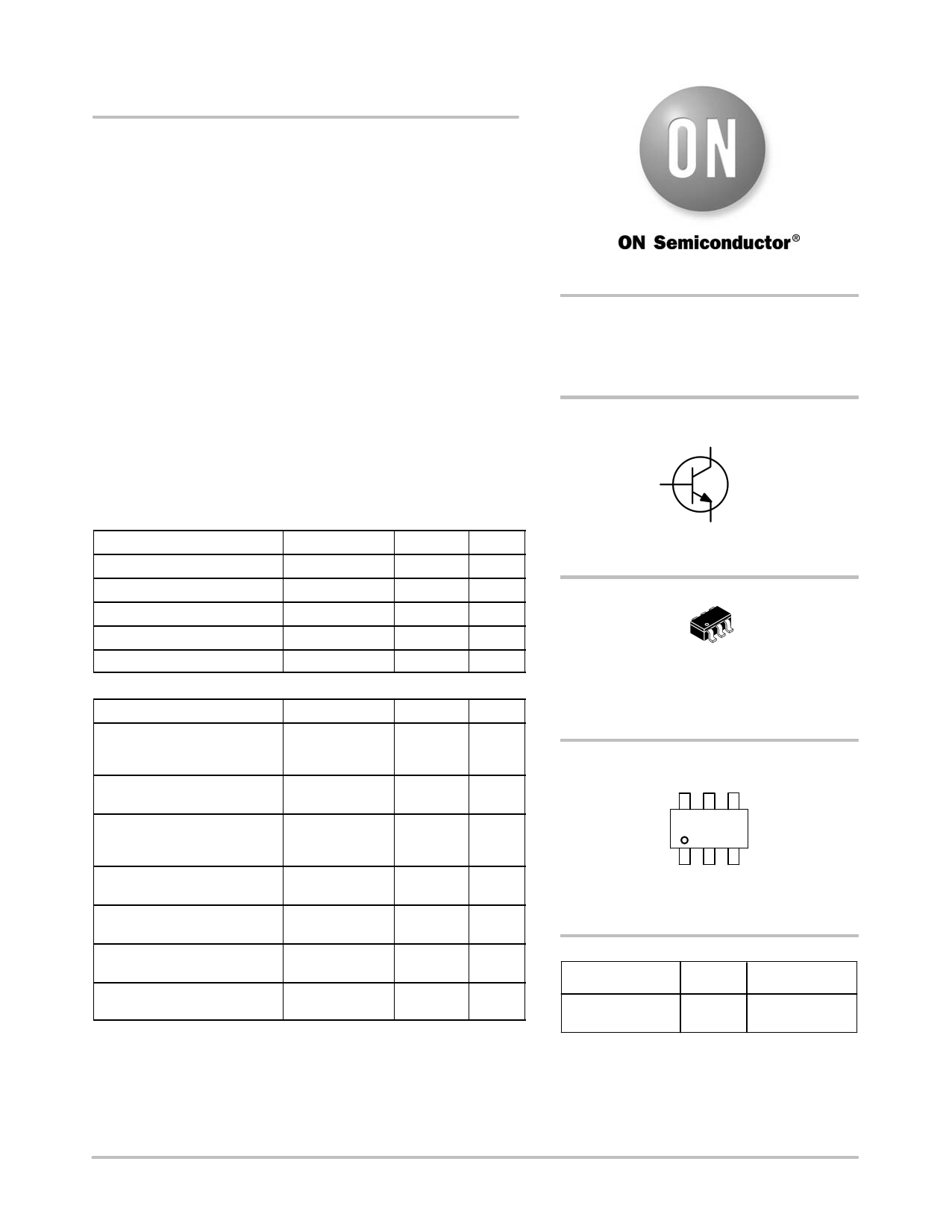
| Logotipo | ||
Hay una vista previa y un enlace de descarga de NSS30201MR6T1G (archivo pdf) en la parte inferior de esta página. Total 6 Páginas | ||
|
No Preview Available !
www.DataSheet4U.com
NSS30201MR6T1G
30 V, 3 A, Low VCE(sat)
NPN Transistor
ON Semiconductor’s e2PowerEdge family of low VCE(sat)
transistors are miniature surface mount devices featuring ultra low
saturation voltage (VCE(sat)) and high current gain capability. These
are designed for use in low voltage, high speed switching applications
where affordable efficient energy control is important.
Typical application are DC−DC converters and power management
in portable and battery powered products such as cellular and cordless
phones, PDAs, computers, printers, digital cameras and MP3 players.
Other applications are low voltage motor controls in mass storage
products such as disc drives and tape drives. In the automotive
industry they can be used in air bag deployment and in the instrument
cluster. The high current gain allows e2PowerEdge devices to be
driven directly from PMU’s control outputs, and the Linear Gain
(Beta) makes them ideal components in analog amplifiers.
• This is a Pb−Free Device
MAXIMUM RATINGS (TA = 25°C)
Rating
Symbol
Max Unit
Collector-Emitter Voltage
Collector-Base Voltage
Emitter-Base Voltage
Collector Current − Continuous
Collector Current − Peak
THERMAL CHARACTERISTICS
VCEO
VCBO
VEBO
IC
ICM
30 V
50 V
5.0 V
2.0 A
3.0 A
Characteristic
Symbol
Max Unit
Total Device Dissipation
TA = 25°C
Derate above 25°C
PD (Note 1)
535 mW
4.3 mW/°C
Thermal Resistance,
Junction−to−Ambient
RqJA (Note 1)
234 °C/W
Total Device Dissipation
TA = 25°C
Derate above 25°C
PD (Note 2)
1.180
9.4
W
mW/°C
Thermal Resistance,
Junction−to−Ambient
RqJA (Note 2)
106 °C/W
Thermal Resistance,
Junction−to−Lead #1
Total Device Dissipation
(Single Pulse < 10 s)
RqJL (Note 1)
RqJL (Note 2)
PDsingle
(Notes 2 and 3)
110
50
1.75
°C/W
°C/W
W
Junction and Storage
Temperature Range
TJ, Tstg
−55 to
+150
°C
Maximum ratings are those values beyond which device damage can occur.
Maximum ratings applied to the device are individual stress limit values (not
normal operating conditions) and are not valid simultaneously. If these limits are
exceeded, device functional operation is not implied, damage may occur and
reliability may be affected.
1. FR−4 with 1 oz and 3.9 mm2 of copper area.
2. FR−4 with 1 oz and 645 mm2 of copper area.
3. Refer to Figure 8.
© Semiconductor Components Industries, LLC, 2005
June, 2005 − Rev. 0
1
http://onsemi.com
30 VOLTS
3.0 AMPS
NPN LOW VCE(sat) TRANSISTOR
EQUIVALENT RDS(on) 100 mW
COLLECTOR
1, 2, 5, 6
3
BASE
4
EMITTER
6 54
1 23
TSOP−6
CASE 318G
STYLE 6
DEVICE MARKING
VS7M
VS7 = Specific Device Code
M = Date Code
ORDERING INFORMATION
Device
Package
Shipping†
NSS30201MR6T1G TSOP−6 3000/Tape & Reel
(Pb−Free)
†For information on tape and reel specifications,
including part orientation and tape sizes, please
refer to our Tape and Reel Packaging Specifications
Brochure, BRD8011/D.
Publication Order Number:
NSS30201MR6/D
1 page 
NSS30201MR6T1G
PACKAGE DIMENSIONS
TSOP−6
CASE 318G−02
ISSUE P
D
65 4
HE
12 3
E
b
e
0.05 (0.002)
A1
A
NOTES:
1. DIMENSIONING AND TOLERANCING PER
ANSI Y14.5M, 1982.
2. CONTROLLING DIMENSION: MILLIMETER.
3. MAXIMUM LEAD THICKNESS INCLUDES LEAD
FINISH THICKNESS. MINIMUM LEAD
THICKNESS IS THE MINIMUM THICKNESS OF
BASE MATERIAL.
4. DIMENSIONS A AND B DO NOT INCLUDE
MOLD FLASH, PROTRUSIONS, OR GATE
BURRS.
q
c
L
MILLIMETERS
DIM MIN NOM MAX
A 0.90
1.00
1.10
A1 0.01
0.06
0.10
b 0.25 0.38 0.50
c 0.10 0.18 0.26
D 2.90
3.00
3.10
E 1.30
1.50
1.70
e 0.85 0.95 1.05
L 0.20 0.40 0.60
H E 2.50
q 0°
2.75
−
3.00
10°
MIN
0.035
0.001
0.010
0.004
0.114
0.051
0.034
0.008
0.099
0°
INCHES
NOM
0.039
0.002
0.014
0.007
0.118
0.059
0.037
0.016
0.108
−
MAX
0.043
0.004
0.020
0.010
0.122
0.067
0.041
0.024
0.118
10°
STYLE 6:
PIN 1. COLLECTOR
2. COLLECTOR
3. BASE
4. EMITTER
5. COLLECTOR
6. COLLECTOR
SOLDERING FOOTPRINT*
2.4
0.094
1.9
0.075
0.95
0.037
0.95
0.037
0.7
0.028
1.0
0.039
ǒ ǓSCALE 10:1
mm
inches
*For additional information on our Pb−Free strategy and soldering
details, please download the ON Semiconductor Soldering and
Mounting Techniques Reference Manual, SOLDERRM/D.
http://onsemi.com
5
5 Page | ||
| Páginas | Total 6 Páginas | |
| PDF Descargar | [ Datasheet NSS30201MR6T1G.PDF ] | |
Hoja de datos destacado
| Número de pieza | Descripción | Fabricantes |
| NSS30201MR6T1G | Low VCE(sat) NPN Transistor | ON Semiconductor |
| Número de pieza | Descripción | Fabricantes |
| SLA6805M | High Voltage 3 phase Motor Driver IC. |
Sanken |
| SDC1742 | 12- and 14-Bit Hybrid Synchro / Resolver-to-Digital Converters. |
Analog Devices |
|
DataSheet.es es una pagina web que funciona como un repositorio de manuales o hoja de datos de muchos de los productos más populares, |
| DataSheet.es | 2020 | Privacy Policy | Contacto | Buscar |