|
|
PDF NCP5181 Data sheet ( Hoja de datos )
| Número de pieza | NCP5181 | |
| Descripción | High Voltage High and Low Side Driver | |
| Fabricantes | ON Semiconductor | |
| Logotipo | ||
Hay una vista previa y un enlace de descarga de NCP5181 (archivo pdf) en la parte inferior de esta página. Total 12 Páginas | ||
|
No Preview Available !
www.DataSheet4U.com
NCP5181
High Voltage High and Low
Side Driver
The NCP5181 is a High Voltage Power MOSFET Driver providing
two outputs for direct drive of 2 N−channel power MOSFETs arranged
in a half−bridge (or any other high−side + low−side) configuration.
It uses the bootstrap technique to insure a proper drive of the
High−side power switch. The driver works with 2 independent inputs
to accommodate any topology (including half−bridge, asymmetrical
half−bridge, active clamp and full−bridge…).
Features
• High Voltage Range: up to 600 V
• dV/dt Immunity ±50 V/nsec
• Gate Drive Supply Range from 10 V to 20 V
• High and Low DRV Outputs
• Output Source / Sink Current Capability 1.1 A / 2.4 A
• 3.3 V and 5 V Input Logic Compatible
• Up to VCC Swing on Input Pins
• Matched Propagation Delays between Both Channels
• Outputs in Phase with the Inputs
• Independent Logic Inputs to Accommodate All Topologies
• Under VCC LockOut (UVLO) for Both Channels
• Pin to Pin Compatible with IR2181(S)
• These are Pb−Free Devices
Applications
• High Power Energy Management
• Half−bridge Power Converters
• Any Complementary Drive Converters (asymmetrical half−bridge,
active clamp)
• Full−bridge Converters
• Bridge Inverters for UPS Systems
PIN ASSIGNMENT
PIN FUNCTION
IN_HI
Logic Input for High Side Driver Output In Phase
IN_LO
Logic Input for Low Side Driver Output In Phase
GND
Ground
DRV_LO
Low Side Gate Drive Output
VCC
VBOOT
DRV_HI
Low Side and Main Power Supply
Bootstrap Power Supply
High Side Gate Drive Output
BRIDGE
Bootstrap Return or High Side Floating Supply Return
http://onsemi.com
IN_HI
IN_LO
GND
DRV_LO
VBOOT
DRV_HI
BRIDGE
VCC
8
1
SOIC−8
D SUFFIX
CASE 751
PDIP−8
P SUFFIX
CASE 626
MARKING DIAGRAMS
8
5181
ALYWX
G
1
NCP5181P
AWL
YYWWG
NCP5181P,
5181 = Specific Device Code
A = Assembly Location
L = Wafer Lot
Y, YY = Year
W, WW = Work Week
G, G = Pb−Free Package
ORDERING INFORMATION
Device
Package
Shipping†
NCP5181PG
NCP5181DR2G
PDIP−8
(Pb−Free)
SOIC−8
(Pb−Free)
50 Units/Tube
2.500/Tape & Reel
†For information on tape and reel specifications,
including part orientation and tape sizes, please
refer to our Tape and Reel Packaging Specification
Brochure, BRD8011/D.
© Semiconductor Components Industries, LLC, 2006
March, 2006 − Rev. 2
1
Publication Order Number:
NCP5181/D
1 page 
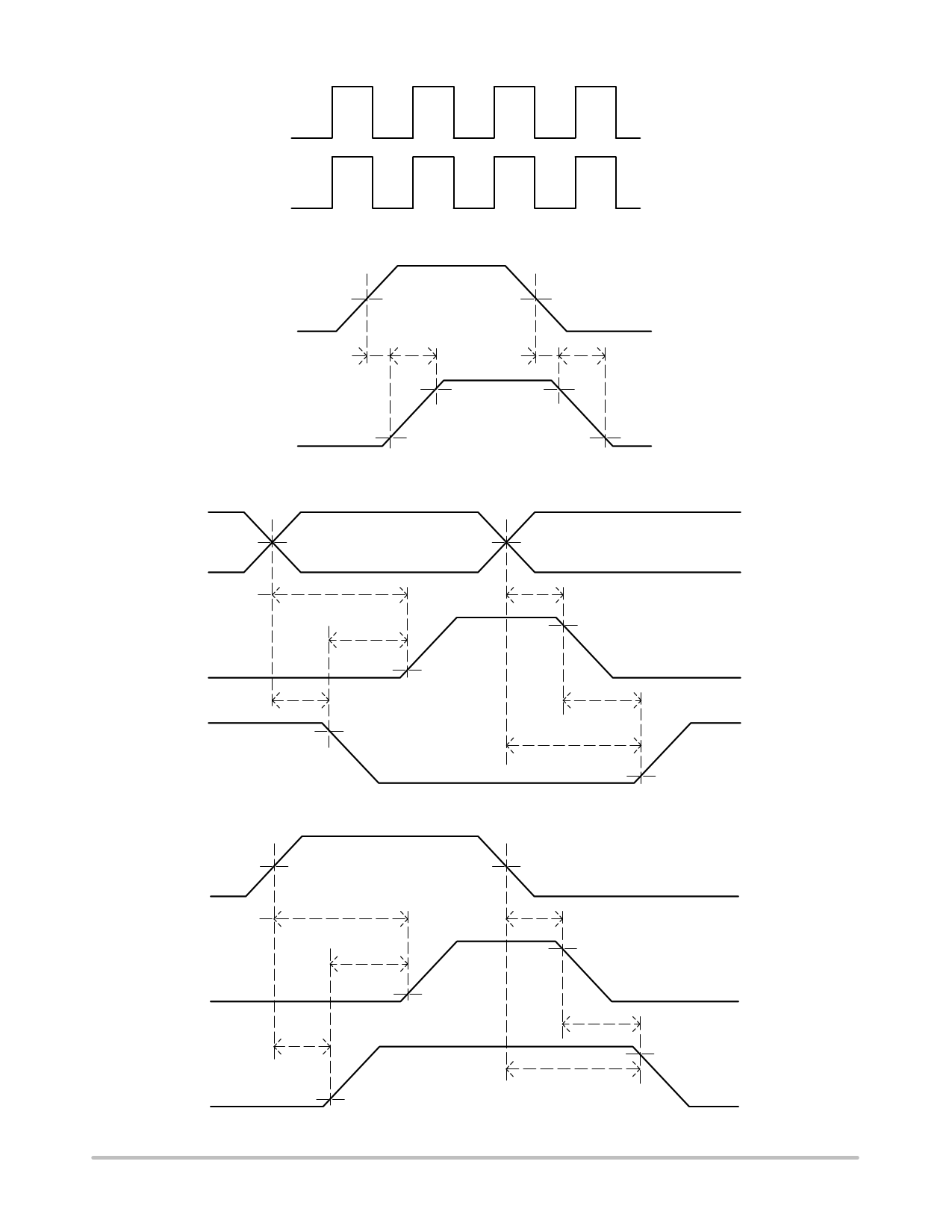
IN_HI
IN_LO
DRV_HI
DRV_LO
NCP5181
Figure 3. Input/Output Timing Diagram
IN_HI
IN_LO
ton
50%
tr
50%
toff
tf
DRV_HI
DRV_LO
90%
90%
10%
10%
Figure 4. Switching Time Waveform Definitions
IN_LO
IN_HI
50%
ton
50%
toff
Delta_t
DRV_HI
toff
10%
90%
Delta_t
DRV_LO
90%
ton
Figure 5. Delay Matching Waveforms Definition
10%
IN_LO
&
IN_HI
50%
ton_HI
50%
toff_HI
Delta_t
90%
DRV_HI
DRV_LO
ton_LO
10%
Delta_t
ton_LO
90%
10%
Figure 6. Other Delay Matching Waveforms Definition
http://onsemi.com
5
5 Page 
NCP5181
−X−
A
PACKAGE DIMENSIONS
SOIC−8 NB
CASE 751−07
ISSUE AG
B
−Y−
−Z−
H
85
S 0.25 (0.010) M Y M
1
4
K
G
D
C
SEATING
PLANE
N X 45 _
0.10 (0.004)
M
0.25 (0.010) M Z Y S X S
J
NOTES:
1. DIMENSIONING AND TOLERANCING PER
ANSI Y14.5M, 1982.
2. CONTROLLING DIMENSION: MILLIMETER.
3. DIMENSION A AND B DO NOT INCLUDE
MOLD PROTRUSION.
4. MAXIMUM MOLD PROTRUSION 0.15 (0.006)
PER SIDE.
5. DIMENSION D DOES NOT INCLUDE DAMBAR
PROTRUSION. ALLOWABLE DAMBAR
PROTRUSION SHALL BE 0.127 (0.005) TOTAL
IN EXCESS OF THE D DIMENSION AT
MAXIMUM MATERIAL CONDITION.
6. 751−01 THRU 751−06 ARE OBSOLETE. NEW
STANDARD IS 751−07.
MILLIMETERS
INCHES
DIM MIN MAX MIN MAX
A 4.80 5.00 0.189 0.197
B 3.80 4.00 0.150 0.157
C 1.35 1.75 0.053 0.069
D 0.33 0.51 0.013 0.020
G 1.27 BSC 0.050 BSC
H 0.10 0.25 0.004 0.010
J 0.19 0.25 0.007 0.010
K 0.40 1.27 0.016 0.050
M 0_ 8_ 0_ 8_
N 0.25 0.50 0.010 0.020
S 5.80 6.20 0.228 0.244
SOLDERING FOOTPRINT*
1.52
0.060
7.0
0.275
4.0
0.155
0.6
0.024
1.270
0.050
ǒ ǓSCALE 6:1
mm
inches
*For additional information on our Pb−Free strategy and soldering
details, please download the ON Semiconductor Soldering and
Mounting Techniques Reference Manual, SOLDERRM/D.
http://onsemi.com
11
11 Page | ||
| Páginas | Total 12 Páginas | |
| PDF Descargar | [ Datasheet NCP5181.PDF ] | |
Hoja de datos destacado
| Número de pieza | Descripción | Fabricantes |
| NCP5181 | High Voltage High and Low Side Driver | ON Semiconductor |
| Número de pieza | Descripción | Fabricantes |
| SLA6805M | High Voltage 3 phase Motor Driver IC. |
Sanken |
| SDC1742 | 12- and 14-Bit Hybrid Synchro / Resolver-to-Digital Converters. |
Analog Devices |
|
DataSheet.es es una pagina web que funciona como un repositorio de manuales o hoja de datos de muchos de los productos más populares, |
| DataSheet.es | 2020 | Privacy Policy | Contacto | Buscar |
