|
|
|
PDF NCP4896 Data sheet ( Hoja de datos )
| Número de pieza | NCP4896 | |
| Descripción | Audio Power Amplifier | |
| Fabricantes | ON Semiconductor | |
| Logotipo | ||
Hay una vista previa y un enlace de descarga de NCP4896 (archivo pdf) en la parte inferior de esta página. Total 16 Páginas | ||
|
No Preview Available !
www.DataSheet4U.com
NCP4896
1.0 Watt Audio Power
Amplifier with Earpiece
Driving Capability
The NCP4896 is an audio power amplifier designed for portable
communication device applications such as mobile phones. This part
is capable of delivering 1.0 W of continuous average power to an
8.0 W BTL load from a 5.0 V power supply and, 250 mW to a 4.0 W
BTL from 2.6 V power supply. It also provides the control of driving
a single−ended earpiece and delivers 90 mW from a 5.0 V power
supply to a 32 W load.
This device provides high quality audio while requiring few
external components and minimal power consumption. It features a
low−power consumption shutdown mode, which is achieved by
driving the shutdown pin with logic Low.
The NCP4896 contains circuitry to prevent from “pop and click”
noise that would otherwise occur during turn−on and turn−off
transitions. It is also efficient when switching modes from BTL to SE
and SE to BTL.
For maximum flexibility, the part provides an externally controlled
gain (with resistors), as well as an externally controlled turn−on time
(with bypass capacitor).
Due to its excellent PSRR, it can be directly connected to the
battery, saving the use of an LDO.
Features
• Single−Ended or Differential Control
• 1.0 W to an 8.0 W BTL Load from a 5.0 V Power Supply
• Excellent PSRR: Direct Connection to the Battery
• Ultra Low Current Shutdown Mode
• 2.2 V−5.5 V Operation
• External Gain Configuration Capability
• External Turn−on Time Configuration Capability
• Thermal Overload Protection Circuitry
• Up to 1.0 nF Capacitive Load Driving Capability
• “Pop and Click” Noise Protection Circuit
• This is a Pb−Free Device
Typical Applications
• Portable Electronic Devices
• PDAs
• Mobile Phones
http://onsemi.com
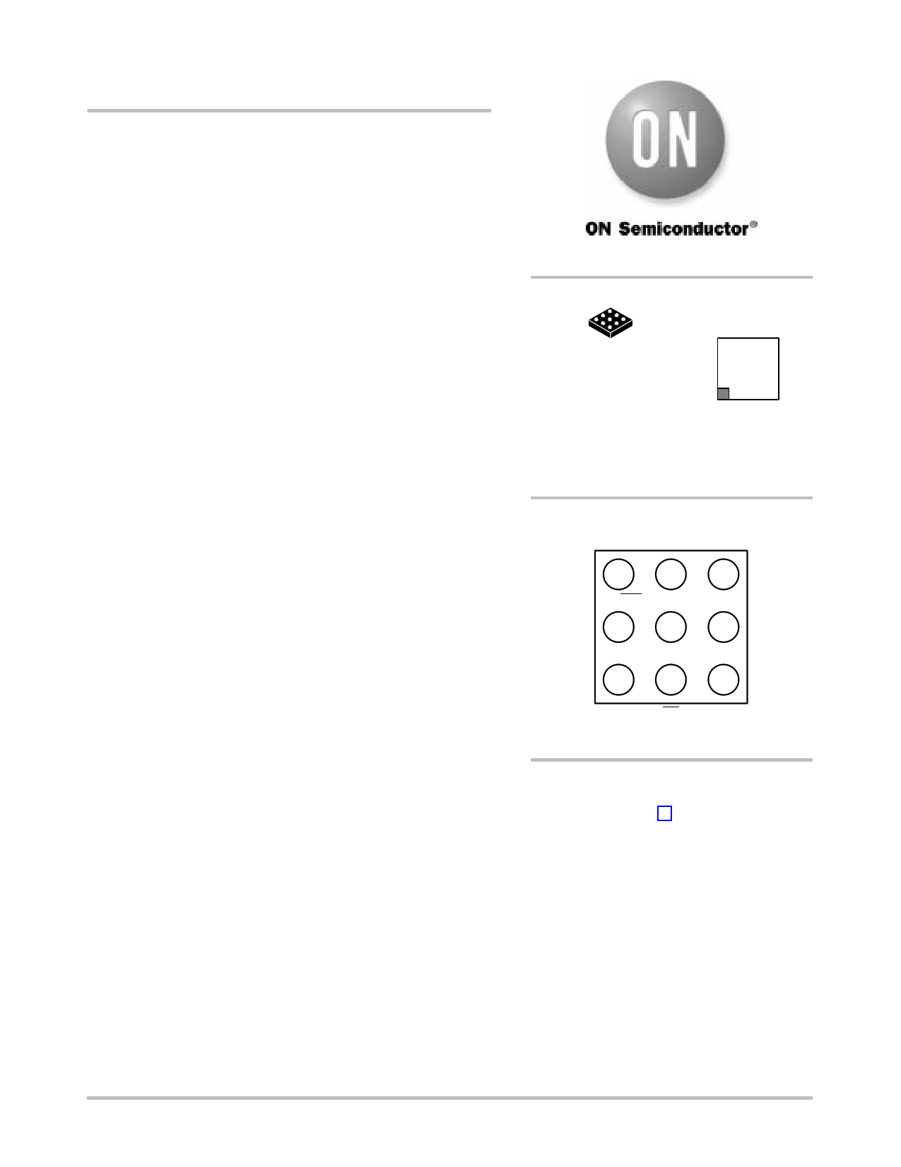
MARKING
DIAGRAM
1
9−PIN FLIP−CHIP
FC SUFFIX
CASE 499AL
A3
XXX
AYWW
A1
C1
XXX
A
Y
WW
= Specific Device Code
= Assembly Location
= Year
= Work Week
PIN CONNECTIONS
9−PIN FLIP−CHIP CSP
A1 A2
SE/BTL BYP
B1 B2
VP NC
C1 C2
A3
OUTB
B3
VM
C3
INM SD OUTA
(Top View)
ORDERING INFORMATION
See detailed ordering and shipping information in the package
dimensions section on page 15 of this data sheet.
© Semiconductor Components Industries, LLC, 2005
March, 2005 − Rev. 3
1
Publication Order Number:
NCP4896/D
1 page 
NCP4896
TYPICAL PERFORMANCE CHARACTERISTICS
10 10
VP = 5.0 V
1 RF = Ri = 20 kW
BTL Mode
RL = 8 W
f = 1.0 kHz
0.1
VP = 3.0 V
1 RF = Ri = 20 kW
BTL Mode
RL = 8 W
f = 1.0 kHz
0.1
0.01
0.001
0
200 400 600 800 1000 1200
Pout, POWER OUT (mW)
Figure 2. THD + N vs. Power Out
(BTL Mode)
10
VP = 2.6 V
RF = Ri = 20 kW
BTL Mode
1 RL = 4 W
f = 1.0 kHz
0.01
0.001
0
1
0.1
100 200 300 400
Pout, POWER OUT (mW)
Figure 3. THD + N vs. Power Out
(BTL Mode)
VP = 5.0 V
RF = Ri = 20 kW
BTL Mode
RL = 8 W
Pout = 250 mW
500
0.1 0.01
0.01
0
1
0.1
100 200 300 400
Pout, POWER OUT (mW)
Figure 4. THD + N vs. Power Out
(BTL Mode)
VP = 3.0 V
RF = Ri = 20 kW
BTL Mode
RL = 8 W
Pout = 250 mW
0.001
500 10
100
1000
10,000
FREQUENCY (Hz)
Figure 5. THD + N vs. Frequency
(BTL Mode)
100,000
VP = 2.6 V
RF = Ri = 20 kW
BTL Mode
0.1 RL = 8 W
Pout = 100 mW
0.01 0.01
0.001
10
100
1000
10,000
FREQUENCY (Hz)
Figure 6. THD + N vs. Frequency
(BTL Mode)
100,000
0.001
10
100
1000
10,000
FREQUENCY (Hz)
Figure 7. THD + N vs. Frequency
(BTL Mode)
100,000
http://onsemi.com
5
5 Page 
NCP4896
APPLICATION INFORMATION
Detailed Description
The NCP4896 audio amplifier can operate from 2.2 V
until 5.5 V power supply. It delivers 320 mW rms output
power to 4.0 W load (VP = 2.6 V) and 1.0 W rms output
power to 8.0 W load (VP = 5.0 V).
The structure of the NCP4896 is basically composed of
two identical internal power amplifiers. Both are externally
configurable with gain−setting resistors Rin and RF (the
closed−loop gain is fixed by the ratios of these resistors).
So the load is driven differentially through OUTA and
OUTB outputs. This configuration eliminates the need for
an output coupling capacitor.
Internal Power Amplifier
The output Pmos and Nmos transistors of the amplifier
were designed to deliver the output power of the
specifications without clipping. The channel resistance
(Ron) of the Nmos and Pmos transistors does not exceed
0.6 W when they drive current.
The structure of the internal power amplifier is
composed of three symmetrical gain stages, first and
medium gain stages are transconductance gain stages to
obtain maximum bandwidth and DC gain.
Turn−On and Turn−Off Transitions
A cycle with a turn−on and turn−off transition is
illustrated with plots that show both single ended signals on
the previous page.
In order to eliminate “pop and click” noises during
transitions, output power in the load must be slowly
established or cut. When logic high is applied to the
shutdown pin, the bypass voltage begins to rise
exponentially and once the output DC level is around the
common mode voltage, the gain is established slowly
(20 ms). This way to turn−on the device is optimized in
terms of rejection of “pop and click” noises.
A theoretical value of turn−on time at 25°C is given by
the following formula.
Cby: bypass capacitor
R: internal 150 k resistor with a 25% accuracy
Ton = 0.95 * R * Cby
The device has the same behavior when it is turned−off
by a logic low on the shutdown pin. During the shutdown
mode, amplifier outputs are connected to the ground.
However, to cut totally the output audio signal, you only
need to wait for 20 ms.
Shutdown Function
The device enters shutdown mode when the shutdown
signal is low. During the shutdown mode, the Dc quiescent
current of the circuit is typically 10 nA.
Current Limit Circuit
The maximum output power of the circuit
(Porms = 1.0 W, VP = 5.0 V, RL = 8.0 W) requires a peak
current in the load of 500 mA.
In order to limit the excessive power dissipation in the
load when a short−circuit occurs, the current limit in the
load is fixed to 800 mA. The current in the four output MOS
transistors are real−time controlled, and when one current
exceeds 800 mA, the gate voltage of the MOS transistor is
clipped and no more current can be delivered.
Single−Ended Operation
In SE mode, the load is driven from the primary amplifier
output (OUTA). The gain is set by the ration between RF
and Ri.
ǒ ǓSE Gain +
−
Rf
Ri
In this SE mode, an output capacitor (Co) is required to
block the common mode voltage at the output of the
amplifier, thus avoiding DC currents in the load. As for the
high pass filter due to the input capacitor and the Ri resistor,
the load gives with Co another first order high pass filter,
the cut−off frequency of which is given by:
Fc
+
1
2pRL @
Co
SE/BTL Operation
Due to the internal control of each amplifier through
SE/BTL pin, the NCP4896 allows a cost saving for
application which requires to drive a example an 8.0 W
BTL and a 32 W Single−Ended load.
The internal circuitry avoids “pop and click” noises that
could occur in both BTL and Singled−Ended loads during
transitions from SE to BTL and BTL to SE.
http://onsemi.com
11
11 Page | ||
| Páginas | Total 16 Páginas | |
| PDF Descargar | [ Datasheet NCP4896.PDF ] | |
Hoja de datos destacado
| Número de pieza | Descripción | Fabricantes |
| NCP4894 | Differential Audio Power Amplifier | ON Semiconductor |
| NCP4896 | Audio Power Amplifier | ON Semiconductor |
| Número de pieza | Descripción | Fabricantes |
| SLA6805M | High Voltage 3 phase Motor Driver IC. |
Sanken |
| SDC1742 | 12- and 14-Bit Hybrid Synchro / Resolver-to-Digital Converters. |
Analog Devices |
|
DataSheet.es es una pagina web que funciona como un repositorio de manuales o hoja de datos de muchos de los productos más populares, |
| DataSheet.es | 2020 | Privacy Policy | Contacto | Buscar |