|
|
PDF NCP4330 Data sheet ( Hoja de datos )
| Número de pieza | NCP4330 | |
| Descripción | Post Regulation Driver | |
| Fabricantes | ON Semiconductor | |
| Logotipo | ||
Hay una vista previa y un enlace de descarga de NCP4330 (archivo pdf) en la parte inferior de esta página. Total 18 Páginas | ||
|
No Preview Available !
www.DataSheet4U.com
NCP4330
Post Regulation Driver
The NCP4330 houses a dual MOSFET driver intended to be used as
a companion chip in AC−DC or DC−DC multi−output post regulated
power supplies. Being directly fed by the secondary AC signal, the
device keeps power dissipation to the lowest while reducing the
surrounding part count. Furthermore, the implementation of a
N−channel MOSFET gives NCP4330−based applications a significant
advantage in terms of efficiency.
Features
• Undervoltage Lockout
• Thermal Shutdown for Overtemperature Protection
• PWM Operation Synchronized to the Converter Frequency
• High Gate Drive Capability
• Bootstrap for N−MOSFET High−Side Drive
• Over−Lap Management for Soft Switching
• High Efficiency Post−Regulation
• Ideal for Frequencies up to 400 kHz
• This is a Pb−Free Device
http://onsemi.com
MARKING
DIAGRAM
8
1
SO−8
D SUFFIX
CASE 751
8
4330D
ALYW
1
4330D
A
L
Y
W
= Device Number
= Assembly Location
= Wafer Lot
= Year
= Work Week
Typical Applications
• ATX 3V3 Post−Regulation
• Offline SMPS with MAGAMP Post−Regulation
• Multi−Outputs DC−DC Converters
VDD
VDD
Vref, UVDth
Band−Gap
AR2
RST
VDD
Undervoltage Detection
(UVD high if VDD < 4.9 V)
UVD
HS_DRV and
LS_DRV low
RESET Block
Level
Shifter
Buffer
U1
INVERTER
C_ramp
I_ramp
Iramp
U4
2.5 V/1.5 V
+
U3
Iramp
− OR
Hysteresis
VDD Comparator
VDD
AR3
GND
Current
Mirror
Buffer
PIN CONNECTIONS
HS_DRV 1
BST 2
RST 3
BST
C_ramp 4
8 GND
7 LS_DRV
6 VDD
5 I_ramp
HS_DRV
(Top View)
ORDERING INFORMATION
Device
Package
Shipping†
NCP4330DR2G SO−8 2500 / Tape & Reel
(Pb−Free)
†For information on tape and reel specifications,
including part orientation and tape sizes, please
refer to our Tape and Reel Packaging Specification
Brochure, BRD8011/D.
LS_DRV
Figure 1. Block Diagram
© Semiconductor Components Industries, LLC, 2005
August, 2005 − Rev. 0
1
Publication Order Number:
NCP4330/D
1 page 
18
16
14
12
10
8
−25
25
TEMPERATURE (°C)
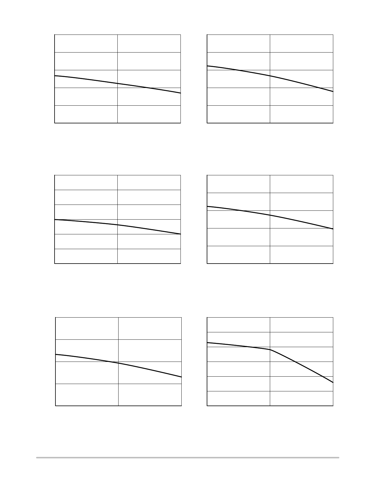
Figure 3. IDD1 Consumption
vs. Temperature
NCP4330
9.0
8.2
7.4
6.6
5.8
5.0
125 −25
25
TEMPERATURE (°C)
Figure 4. IDD2 Consumption
vs. Temperature
125
14
13
12
11
10
9
8
−25
25
TEMPERATURE (°C)
Figure 5. IDD3 Consumption
vs. Temperature
6.0
5.9
5.8
5.7
5.6
5.5
125 −25
25
TEMPERATURE (°C)
125
Figure 6. Undervoltage Lockout Upper
Threshold vs. Temperature
5.22 700
660
5.20
620
5.18 580
540
5.16
500
5.14
−25
25
TEMPERATURE (°C)
460
125 −25
25
TEMPERATURE (°C)
125
Figure 7. Undervoltage Lockout Lower
Threshold vs. Temperature
Figure 8. Undervoltage Lockout Hysteresis
vs. Temperature
http://onsemi.com
5
5 Page 
NCP4330
Low−Side Driver Stage
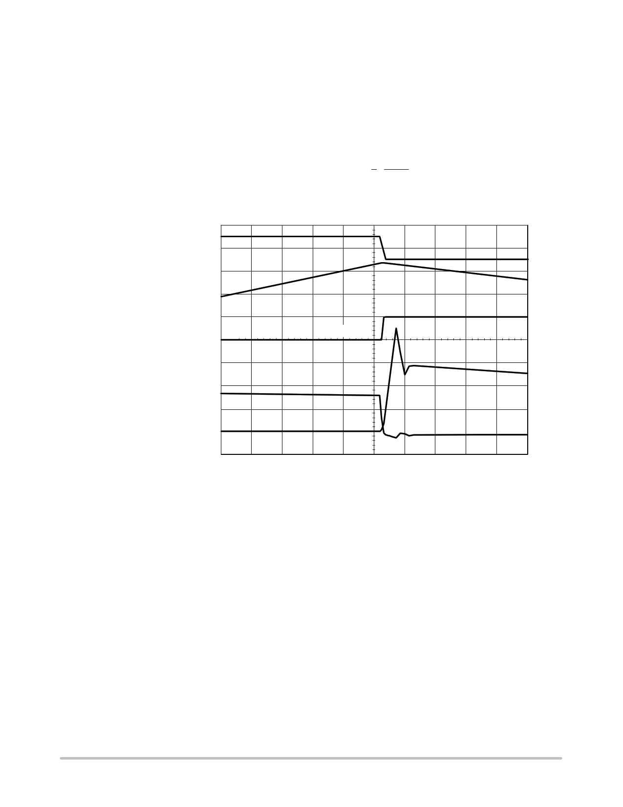
The timing diagram of page 2 portrays the sequencing
driven by the NCP4330.
The low−side drive is controlled by an internal
comparator that compares the C_ramp voltage to the internal
reference 2.5 V (1.0 V hysteresis). When the C_ramp
exceeds the 2.5 V reference, the comparator turns high
forcing the low−side MOSFET off. 100 ns later, the
high−side MOSFET switches on.
When a reset signal is applied to the reset pin, the C_ramp
capacitor is grounded. As a consequence, the internal
comparator turns low and forces the low−side MOSFET on.
100 ns later, the high−side MOSFET switches off.
The low−side drive is designed to drive on and off a 25 nC
gate charge power MOSFET, in 25 ns typical.
1. Low−Side MOSFET Turn On:
In nominal operation, the body diode is already ON when
the low−side MOSFET turns on. The energy Qg to be
supplied is then approximately half the energy necessary if
the drain source voltage was high.
The necessary current capability is then:
Ils
*
on
+
1
2
*
25
25
nC
ns
,
that
is
500
mA.
80.0 0 6.50 16.0 40.0
60.0 −80.0 4.50 12.0 20.0
40.0 −160 2.50 8.00
0
Vin
lind
LS_DRV
vin1
i(l1)
ls_drv
20.0 −240 500 M 4.00 −20.0
irl
IQ
0 −320 −1.50 0 −40.0
VQ
4.5010 M
4.5015 M
4.5020 M
Time in Secs
Figure 28. Low−Side MOSFET Turn ON
4.5025 M
v(vsn)
4.5030 M
http://onsemi.com
11
11 Page | ||
| Páginas | Total 18 Páginas | |
| PDF Descargar | [ Datasheet NCP4330.PDF ] | |
Hoja de datos destacado
| Número de pieza | Descripción | Fabricantes |
| NCP433 | 1.5A Ultra-Small Controlled Load Switch | ON Semiconductor |
| NCP4330 | Post Regulation Driver | ON Semiconductor |
| NCP4331 | Synchronous Buck Controller | ON Semiconductor |
| Número de pieza | Descripción | Fabricantes |
| SLA6805M | High Voltage 3 phase Motor Driver IC. |
Sanken |
| SDC1742 | 12- and 14-Bit Hybrid Synchro / Resolver-to-Digital Converters. |
Analog Devices |
|
DataSheet.es es una pagina web que funciona como un repositorio de manuales o hoja de datos de muchos de los productos más populares, |
| DataSheet.es | 2020 | Privacy Policy | Contacto | Buscar |
