|
|
|
PDF NCP1522 Data sheet ( Hoja de datos )
| Número de pieza | NCP1522 | |
| Descripción | Adjustable Output Voltage Step-Down Converter | |
| Fabricantes | ON Semiconductor | |
| Logotipo | ||
Hay una vista previa y un enlace de descarga de NCP1522 (archivo pdf) en la parte inferior de esta página. Total 17 Páginas | ||
|
No Preview Available !
www.DataSheet4U.com
NCP1522
3.0 MHz, 600 mA,
High−Efficiency, Low
Quiescent Current,
Adjustable Output Voltage
Step−Down Converter
The NCP1522 step−down PWM DC−DC converter is optimized
for portable applications powered from one cell Li−ion or three cell
Alkaline/NiCd/NiMH batteries. The device is available in an
adjustable output voltage from 0.9 V to 3.3 V. It uses synchronous
rectification to increase efficiency and reduce external part count.
The device also has a built−in 3.0 MHz (nominal) oscillator which
reduces component size by allowing a small inductor and capacitors.
Automatic switching PWM/PFM mode offers improved system
efficiency.
Finally, it includes an integrated soft−start, cycle−by−cycle current
limiting, and thermal shutdown protection. The NCP1522 is
available in a space saving, low profile TSOP5 package.
Features
• 93.8% of Efficiency for 3.3 V Output and 4.5 V Input and 120 mA
Load Current
• Sources up to 600 mA
• 3.0 MHz Switching Frequency
• Adjustable Output Voltage from 0.9 V to 3.3 V
• 60 mA Quiescent Current (Typ)
• Synchronous Rectification for Higher Efficiency
• 2.7 V to 5.5 V Input Voltage Range
• Thermal Limit Protection
• Shutdown Current Consumption of 0.3 mA
• Short Circuit Protection
• This is a Pb−Free Device
Typical Applications
• Cellular Phones, Smart Phones and PDAs
• MP3 Players and Portable Audio Systems
• Wireless and DSL Modems
• Portable Equipment
• USB Powered Devices
• Digital Still/Video Cameras
http://onsemi.com
5
1
TSOP−5
ASN SUFFIX
CASE 483
MARKING
DIAGRAM
5
DBRAYWG
G
1
A = Assembly Location
Y = Year
W = Work Week
G = Pb−Free Package
(Note: Microdot may be in either location)
PIN CONNECTIONS
VIN 1
GND 2
EN 3
5 LX
4 FB
(Top View)
ORDERING INFORMATION
Device
Package
Shipping
NCP1522ASNT1G TSOP−5 3000/Tape & Reel
(Pb−Free)
†For information on tape and reel specifications,
including part orientation and tape sizes, please
refer to our Tape and Reel Packaging Specification
Brochure, BRD8011/D.
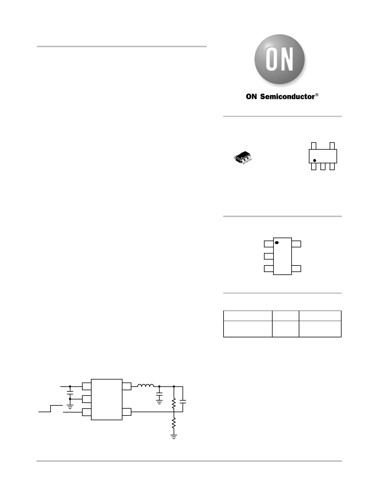
VIN
CIN
OFF ON
1 VIN LX 5
2 GND
3 EN
FB 4
L
COUT
VOUT
R1 Cff
R2
Figure 1. Typical Application
© Semiconductor Components Industries, LLC, 2006
August, 2006 − Rev. 3
1
Publication Order Number:
NCP1522/D
1 page 
NCP1522
100
90
80
70
60
50
40
30
20
10
0
2.7
EN = VIN
IOUT = 0 mA
3.2 3.7 4.2 4.7
VIN, INPUT VOLTAGE (V)
5.2
5.7
Figure 4. Quiescent Current vs. Supply Voltage
100
90
80
70
60
50
40
30
20
10
0
−40
−20
VIN = 5.5 V
VIN = 2.7 V
0 20 40 60
TEMPERATURE (°C)
80 100
Figure 5. Quiescent Current vs. Temperature
1.0
EN = 0 V
0.8 IOUT = 0 mA
0.6
0.4
0.2
0
2.7 3.2 3.7 4.2 4.7
VIN, INPUT VOLTAGE (V)
Figure 6. Shutdown Current vs. Supply Voltage
100
95
90 TA = −40°C
TA = 25°C
85
80
75 TA = 85°C
70
0 100 200 300 400 500 600
IOUT, OUTPUT CURRENT (mA)
Figure 7. Efficiency vs. Output Current
(VOUT = 1.8 V, VIN = 3.6 V)
100 100
90
TA = −40°C
80
TA = 25°C
70
60
TA = 85°C
50
0 100 200 300 400 500 600
IOUT, OUTPUT CURRENT (mA)
Figure 8. Efficiency vs. Output Current
(VOUT = 0.9 V, VIN = 3.6 V)
TA = −40°C
90
TA = 25°C
TA = 85°C
80
70
0 100 200 300 400 500 600
IOUT, OUTPUT CURRENT (mA)
Figure 9. Efficiency vs. Output Current
(VOUT = 3.3 V, VIN = 4.5 V)
http://onsemi.com
5
5 Page 
NCP1522
APPLICATION INFORMATION
Output Voltage Selection
The output voltage is programmed through an external
resistor divider connected from VOUT to FB then to GND.
For low power consumption and noise immunity, the
resistor from FB to GND (R2) should be in the
[100 k−600 k] range. If R2 is 200 k given the VFB is 0.6 V,
the current through the divider will be 3.0 mA.
The formula below gives the value of VOUT, given the
desired R1 and the R1 value:
VOUT + VFB (1 ) RR12)
• VOUT: Output Voltage (Volts)
• VFB: Feedback Voltage = 0.6 V
• R1: Feedback Resistor from VOUT to FB
• R2: Feedback Resistor from FB to GND
(eq. 2)
Input Capacitor Selection
In PWM operating mode, the input current is pulsating
with large switching noise. Using an input bypass capacitor
can reduce the peak current transients drawn from the
input supply source, thereby reducing switching noise
significantly. The capacitance needed for the input bypass
capacitor depends on the source impedance of the input
supply.
The maximum RMS current occurs at 50% duty cycle
with maximum output current, which is IO, max/2.
For NCP1522, a low profile, low ESR ceramic capacitor
of 4.7 mF should be used for most of the cases. For effective
bypass results, the input capacitor should be placed as close
as possible to the VIN pin.
Table 1. List of Input Capacitor
Murata
GRM188R60J475KE
GRM21BR71C475KA
Taiyo Yuden
JMK212BY475MG
TDK
C2012X5ROJ475KB
C1632X5ROJ475KT
Output L−C Filter Design Considerations
The NCP1522 is built in 3.0 MHz frequency and uses
voltage mode architecture. The correct selection of the
output filter ensures good stability and fast transient
response.
Due to the nature of the buck converter, the output L−C
filter must be selected to work with internal compensation.
For NCP1522, the internal compensation is internally fixed
and it is optimized for an output filter of L = 2.2 mH and
COUT = 4.7 mF.
The corner frequency is given by:
fc + 2p ǸL
1
COUT
+
2p
Ǹ2.2
1
mH
+ 49.5 kHz
4.7 mF
(eq. 3)
The device is intended to operate with inductance
between 1.0 mH and maximum of 4.7 mH.
If the corner frequency is moved, it is recommended to
check the loop stability depending on the output ripple
voltage accepted and output current required. For lower
frequency, the stability will be increased; a larger output
capacitor value could be chosen without critical effect on
the system. On the other hand, a smaller capacitor value
increases the corner frequency and it should be critical for
the system stability. Take care to check the loop stability.
The phase margin is usually higher than 45°.
Table 2. L−C Filter Example
Inductance (L)
1.0 mH
2.2 mH
4.7 mH
Output Capacitor (Cout)
10 mF
4.7 mF
2.2 mF
Inductor Selection
The inductor parameters directly related to device
performances are saturation current and DC resistance and
inductance value. The inductor ripple current (ÄIL)
decreases with higher inductance:
ǒ ǓDIL
+
VOUT
L fSW
1−
VOUT
VIN
(eq. 4)
DIL peak to peak inductor ripple current
L inductor value
fSW switching frequency
The saturation current of the inductor should be rated
higher than the maximum load current plus half the ripple
current:
IL(MAX)
+
IO(MAX)
)
DIL
2
(eq. 5)
IL(MAX) Maximum Inductor Current
IO(MAX) Maximum Output Current
The inductor’s resistance will factor into the overall
efficiency of the converter. For best performances, the DC
resistance should be less than 0.3 W for good efficiency.
http://onsemi.com
11
11 Page | ||
| Páginas | Total 17 Páginas | |
| PDF Descargar | [ Datasheet NCP1522.PDF ] | |
Hoja de datos destacado
| Número de pieza | Descripción | Fabricantes |
| NCP152 | Low Dropout Voltage Regulator | ON Semiconductor |
| NCP1521 | Adjustable Output Voltage Step-Down Converter | ON Semiconductor |
| NCP1521B | Step-Down DC-DC Converter | ON Semiconductor |
| NCP1522 | Adjustable Output Voltage Step-Down Converter | ON Semiconductor |
| Número de pieza | Descripción | Fabricantes |
| SLA6805M | High Voltage 3 phase Motor Driver IC. |
Sanken |
| SDC1742 | 12- and 14-Bit Hybrid Synchro / Resolver-to-Digital Converters. |
Analog Devices |
|
DataSheet.es es una pagina web que funciona como un repositorio de manuales o hoja de datos de muchos de los productos más populares, |
| DataSheet.es | 2020 | Privacy Policy | Contacto | Buscar |