|
|
|
PDF ADUM1210 Data sheet ( Hoja de datos )
| Número de pieza | ADUM1210 | |
| Descripción | Dual-Channel Digital Isolator | |
| Fabricantes | Analog Devices | |
| Logotipo | ||
Hay una vista previa y un enlace de descarga de ADUM1210 (archivo pdf) en la parte inferior de esta página. Total 16 Páginas | ||
|
No Preview Available !
www.DataSheet4U.com
FEATURES
Narrow body, 8-lead SOIC
Low power operation
5 V operation
1.1 mA per channel maximum @ 0 Mbps to 2 Mbps
3.7 mA per channel maximum @ 10 Mbps
3 V operation
0.8 mA per channel maximum @ 0 Mbps to 2 Mbps
2.2 mA per channel maximum @ 10 Mbps
3 V/5 V level translation
High temperature operation: 105°C
High data rate: dc to 25 Mbps (NRZ)
Precise timing characteristics
3 ns maximum pulse width distortion
3 ns maximum channel-to-channel matching
High common-mode transient immunity: >25 kV/μs
Safety and regulatory approvals
UL recognition
2500 V rms for 1 minute per UL 1577
CSA Component Acceptance Notice #5A
VDE certificate of conformity
DIN EN 60747-5-2 (VDE 0884 Part 2): 2003-01
DIN EN 60950 (VDE 0805): 2001-12; DIN EN 60950: 2000
VIORM = 560 V peak
APPLICATIONS
Size-critical multichannel isolation
SPI® interface/data converter isolation
RS-232/RS-422/RS-485 transceiver isolation
Digital field bus isolation
Dual-Channel Digital Isolator
ADuM1210
GENERAL DESCRIPTION
The ADuM12101 is a dual-channel, digital isolator based on
Analog Devices’ iCoupler® technology. Combining high speed
CMOS and monolithic transformer technology, this isolation
component provides outstanding performance characteristics
superior to alternatives such as optocoupler devices.
By avoiding the use of LEDs and photodiodes, iCoupler devices
remove the design difficulties commonly associated with
optocouplers. The concerns of the typical optocoupler
regarding uncertain current transfer ratios, nonlinear transfer
functions, and temperature and lifetime effects are eliminated
with the simple, iCoupler digital interfaces and stable
performance characteristics. The need for external drivers and
other discrete components is eliminated with iCoupler products.
Furthermore, iCoupler devices consume one-tenth to one-sixth
the power of optocouplers at comparable signal data rates.
The ADuM1210 isolator provides two independent isolation
channels operable with the supply voltage on either side ranging
from 2.7 V to 5.5 V. This provides compatibility with lower
voltage systems as well as enabling a voltage translation
functionality across the isolation barrier. In addition, the
ADuM1210 provides low pulse-width distortion (<3 ns) and
tight channel-to-channel matching (<3 ns). Unlike other
optocoupler alternatives, the ADuM1210 isolator has a patented
refresh feature that ensures dc correctness in the absence of
input logic transitions and during power-up/power-down
conditions. Furthermore, as an alternative to the ADuM1200
dual-channel, digital isolator that defaults to an output high
condition, the ADuM1210’s outputs default to a logic low state
when input power is off.
1 Protected by U.S. Patents 5,952,849; 6,873,065; and other pending patents.
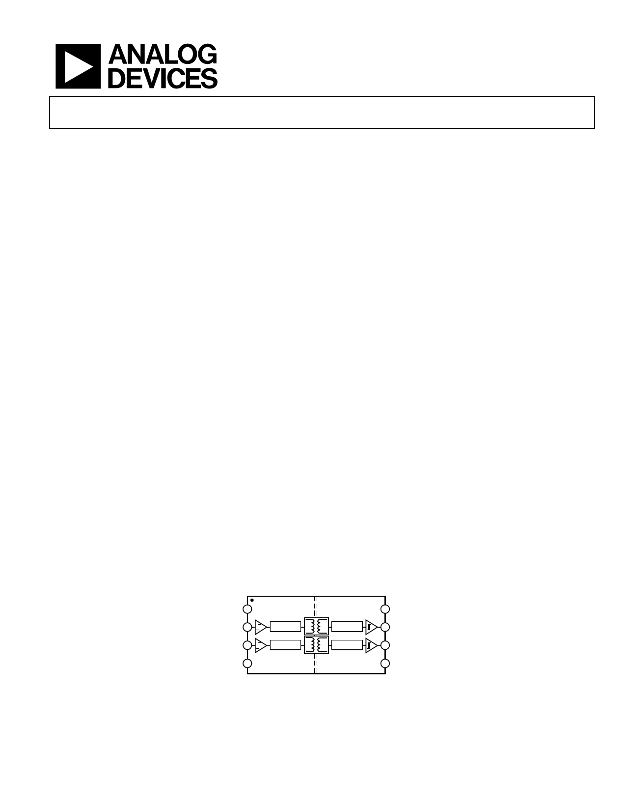
FUNCTIONAL BLOCK DIAGRAM
VDD1 1
VIA 2
VIB 3
GND1 4
ENCODE
ENCODE
DECODE
DECODE
Figure 1.
8 VDD2
7 VOA
6 VOB
5 GND2
Rev. A
Information furnished by Analog Devices is believed to be accurate and reliable. However, no
responsibility is assumed by Analog Devices for its use, nor for any infringements of patents or other
rights of third parties that may result from its use. Specifications subject to change without notice. No
license is granted by implication or otherwise under any patent or patent rights of Analog Devices.
Trademarksandregisteredtrademarksarethepropertyoftheirrespectiveowners.
One Technology Way, P.O. Box 9106, Norwood, MA 02062-9106, U.S.A.
Tel: 781.329.4700
www.analog.com
Fax: 781.461.3113
©2006 Analog Devices, Inc. All rights reserved.
1 page 
ADuM1210
ELECTRICAL CHARACTERISTICS—3 V OPERATION
All voltages are relative to their respective ground. 2.7 V ≤ VDD1 ≤ 3.6 V, 2.7 V ≤ VDD2 ≤ 3.6 V. All minimum/maximum specifications
apply over the entire recommended operating range, unless otherwise noted. All typical specifications are at TA = 25°C, VDD1 = VDD2 = 3.0 V.
Table 2.
Parameter
DC SPECIFICATIONS
Input Supply Current, per Channel, Quiescent
Output Supply Current, per Channel, Quiescent
Total Supply Current, Two Channels1
DC to 2 Mbps
VDD1 Supply Current
VDD2 Supply Current
10 Mbps
VDD1 Supply Current
VDD2 Supply Current
Input Currents
Logic High Input Threshold
Logic Low Input Threshold
Logic High Output Voltages
Logic Low Output Voltages
SWITCHING SPECIFICATIONS
Minimum Pulse Width2
Maximum Data Rate3
Propagation Delay4
Pulse-Width Distortion, |tPLH − tPHL|4
Change vs. Temperature
Propagation Delay Skew5
Channel-to-Channel Matching, Codirectional
Channels6
Channel-to-Channel Matching, Opposing-
Directional Channels6
Output Rise/Fall Time (10% to 90%)
Common-Mode Transient Immunity at
Logic High Output7
Common-Mode Transient Immunity at
Logic Low Output7
Refresh Rate
Input Dynamic Supply Current, per Channel8
Output Dynamic Supply Current, per Channel8
Symbol Min
IDDI (Q)
IDDO (Q)
Typ Max
0.26 0.35
0.11 0.20
Unit
mA
mA
Test Conditions
IDD1 (Q)
IDD2 (Q)
0.6 1.0
0.2 0.6
mA
mA
DC to 1 MHz logic signal freq.
DC to 1 MHz logic signal freq.
IDD1 (10)
IDD2 (10)
IIA, IIB
VIH
VIL
VOAH
VOBH
VOAL
VOBL
−10
0.7 VDD1,
VDD2
VDD1/
VDD2 − 0.1
VDD1/
VDD2 − 0.5
2.2
0.7
+0.01
3.0
2.8
0.0
0.04
0.2
3.4
1.1
+10
0.3 VDD1,
VDD2
0.1
0.1
0.4
mA
mA
μA
V
V
V
V
V
V
V
5 MHz logic signal freq.
5 MHz logic signal freq.
0 ≤ VIA, VIB, ≤ VDD1 or VDD2
IOx = −20 μA, VIx = VIxH
IOx = −4 mA, VIx = VIxH
IOx = 20 μA, VIx = VIxL
IOx = 400 μA, VIx = VIxL
IOx = 4 mA, VIx = VIxL
PW
tPHL, tPLH
PWD
10
20
tPSK
tPSKCD
tPSKOD
tR/tF
|CMH|
|CML|
fr
IDDI (D)
IDDO (D)
25
25
100
60
3
5
22
3
22
3.0
35
35
1.1
0.10
0.03
ns
Mbps
ns
ns
ps/°C
ns
ns
CL = 15 pF, CMOS signal levels
CL = 15 pF, CMOS signal levels
CL = 15 pF, CMOS signal levels
CL = 15 pF, CMOS signal levels
CL = 15 pF, CMOS signal levels
CL = 15 pF, CMOS signal levels
CL = 15 pF, CMOS signal levels
ns CL = 15 pF, CMOS signal levels
ns
kV/μs
kV/μs
Mbps
mA/Mbps
mA/Mbps
CL = 15 pF, CMOS signal levels
VIx = VDD1, VDD2, VCM = 1000 V,
transient magnitude = 800 V
VIx = 0 V, VCM = 1000 V,
transient magnitude = 800 V
Rev. A | Page 5 of 16
5 Page 
ADuM1210
ABSOLUTE MAXIMUM RATINGS
Ambient temperature = 25°C, unless otherwise noted.
Table 9.
Parameter
Storage Temperature
Ambient Operating Temperature
Supply Voltages1
Input Voltage1
Output Voltage1
Average Output Current, per Pin2
Common-Mode Transients3
Symbol
TST
TA
VDD1, VDD2
VIA, VIB
VOA, VOB
IO
CML, CMH
Min
−55
−40
−0.5
−0.5
−0.5
−35
−100
Max
150
105
7.0
VDDI + 0.5
VDDO + 0.5
35
+100
Unit
°C
°C
V
V
V
mA
kV/μs
1 All voltages are relative to their respective ground.
2 See Figure 2 for maximum rated current values for various temperatures.
3 Refers to common-mode transients across the insulation barrier. Common-mode transients exceeding the Absolute Maximum Rating may cause latch-up or
permanent damage.
Stresses above those listed under Absolute Maximum Ratings may cause permanent damage to the device. This is a stress rating only;
Functional operation of the device at these or any other conditions above those listed in the operational sections of this specification is
not implied. Exposure to absolute maximum rating conditions for extended periods may affect device reliability.
Table 10. ADuM1210 Truth Table (Positive Logic)
VIA Input VIB Input VDD1 State VDD2 State
H
H
Powered
Powered
L
L
Powered
Powered
H
L
Powered
Powered
L
H
Powered
Powered
X X Unpowered Powered
VOA Output
H
L
H
L
L
X
X
Powered
Unpowered Indeterminate
VOB Output
H
L
L
H
L
Indeterminate
Notes
Outputs return to the input state within 1 μs
of VDDI power restoration.
Outputs return to the input state within 1 μs
of VDDO power restoration.
ESD CAUTION
ESD (electrostatic discharge) sensitive device. Electrostatic charges as high as 4000 V readily accumulate on
the human body and test equipment and can discharge without detection. Although this product features
proprietary ESD protection circuitry, permanent damage may occur on devices subjected to high energy
electrostatic discharges. Therefore, proper ESD precautions are recommended to avoid performance
degradation or loss of functionality.
Rev. A | Page 11 of 16
11 Page | ||
| Páginas | Total 16 Páginas | |
| PDF Descargar | [ Datasheet ADUM1210.PDF ] | |
Hoja de datos destacado
| Número de pieza | Descripción | Fabricantes |
| ADUM1210 | Dual-Channel Digital Isolator | Analog Devices |
| ADuM121N | Dual-Channel Digital Isolators | Analog Devices |
| Número de pieza | Descripción | Fabricantes |
| SLA6805M | High Voltage 3 phase Motor Driver IC. |
Sanken |
| SDC1742 | 12- and 14-Bit Hybrid Synchro / Resolver-to-Digital Converters. |
Analog Devices |
|
DataSheet.es es una pagina web que funciona como un repositorio de manuales o hoja de datos de muchos de los productos más populares, |
| DataSheet.es | 2020 | Privacy Policy | Contacto | Buscar |