|
|
|
PDF ADT7473 Data sheet ( Hoja de datos )
| Número de pieza | ADT7473 | |
| Descripción | dBCool Remote Thermal Monitor and Fan Controller | |
| Fabricantes | Analog Devices | |
| Logotipo | ||
Hay una vista previa y un enlace de descarga de ADT7473 (archivo pdf) en la parte inferior de esta página. Total 30 Páginas | ||
|
No Preview Available !
www.DataSheet4U.com
dBCool® Remote Thermal
Monitor and Fan Controller
ADT7473
FEATURES
GENERAL DESCRIPTION
Controls and monitors up to 4 fans
High and low frequency fan drive signal
1 on-chip and 2 remote temperature sensors
Series resistance cancellation on the remote channel
Extended temperature measurement range, up to 191°C
Dynamic TMIN control mode optimizes system acoustics
intelligently
Automatic fan speed control mode controls system cooling
based on measured temperature
The ADT7473 dBCool controller is a thermal monitor and
multiple PWM fan controller for noise sensitive or power
sensitive applications requiring active system cooling. The
ADT7473 can drive a fan using either a low or high frequency
drive signal, monitor the temperature of up to two remote
sensor diodes plus its own internal temperature, and measure
and control the speed of up to four fans so they operate at the
lowest possible speed for minimum acoustic noise.
Enhanced acoustic mode dramatically reduces user
perception of changing fan speeds
Thermal protection feature via THERM output
Monitors performance impact of Intel® Pentium®4 processor
Thermal control circuit via THERM input
The automatic fan speed control loop optimizes fan speed for a
given temperature. A unique dynamic TMIN control mode
enables the system thermals/acoustics to be intelligently
managed. The effectiveness of the system’s thermal solution can
be monitored using the THERM input. The ADT7473 also
3-wire and 4-wire fan speed measurement
Limit comparison of all monitored values
Meets SMBus 2.0 electrical specifications
(fully SMBus 1.1 compliant)
provides critical thermal protection to the system using the
bidirectional THERM pin as an output to prevent system or
component overheating.
Fully ROHS compliant
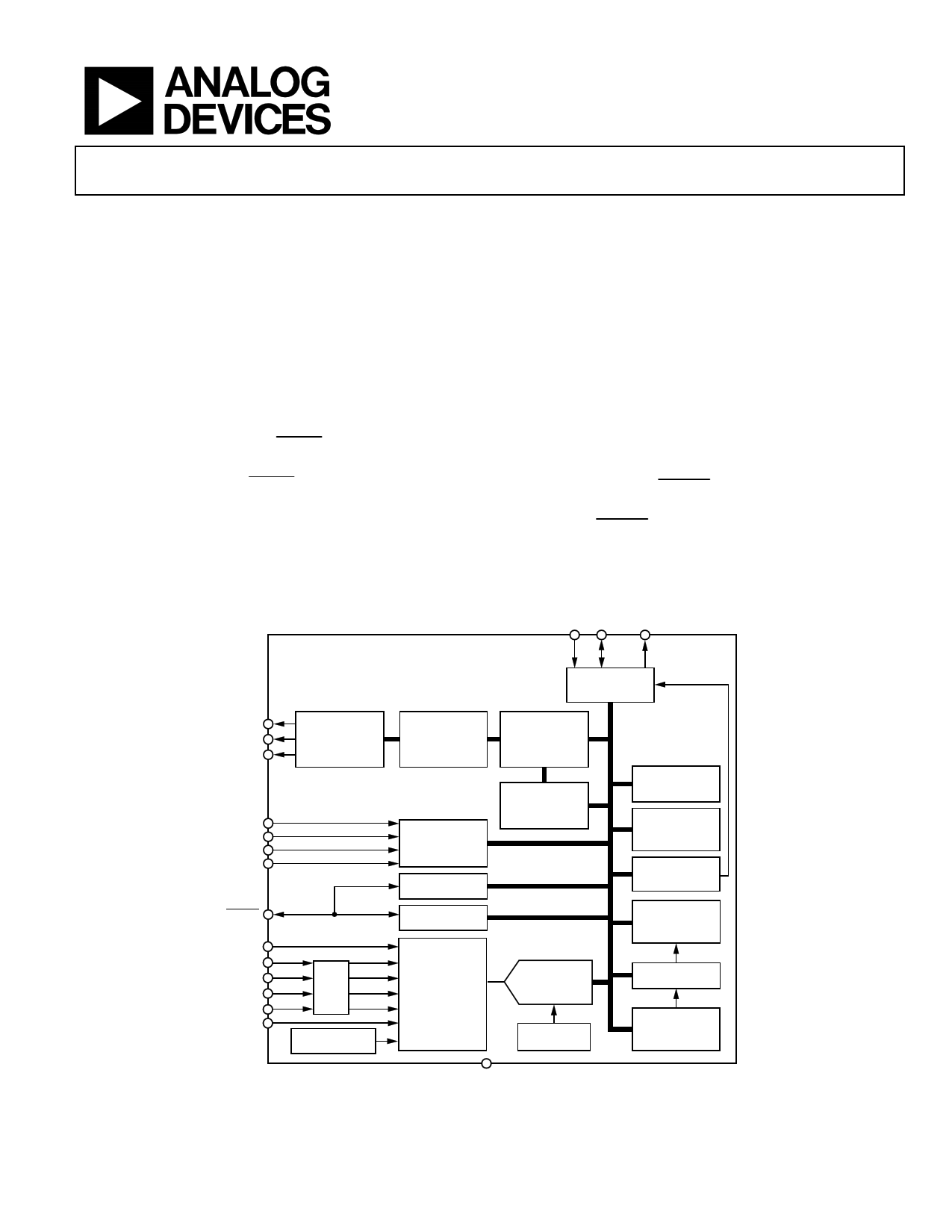
FUNCTIONAL BLOCK DIAGRAM
SCL SDA SMBALERT
ADT7473
SERIAL BUS
INTERFACE
PWM1
PWM2
PWM3
TACH1
TACH2
TACH3
TACH4
THERM
VCC
D1+
D1–
D2+
D2–
VCCP
PWM
REGISTERS
AND
CONTROLLERS
(HF AND LF)
ACOUSTIC
ENHANCEMENT
CONTROL
VCC TO ADT7473
SRC
BAND GAP
TEMP SENSOR
FAN
SPEED
COUNTER
PERFORMANCE
MONITORING
THERMAL
PROTECTION
INPUT
SIGNAL
CONDITIONING
AND
ANALOG
MULTIPLEXER
AUTOMATIC
FAN SPEED
CONTROL
DYNAMIC
TMIN
CONTROL
10-BIT
ADC
BAND GAP
REFERENCE
ADDRESS
POINTER
REGISTER
PWM
CONFIGURATION
REGISTERS
INTERRUPT
MASKING
INTERRUPT
STATUS
REGISTERS
LIMIT
COMPARATORS
VALUE AND
LIMIT
REGISTERS
GND
Figure 1.
Rev. A
Information furnished by Analog Devices is believed to be accurate and reliable. However, no
responsibility is assumed by Analog Devices for its use, nor for any infringements of patents or other
rights of third parties that may result from its use. Specifications subject to change without notice. No
license is granted by implication or otherwise under any patent or patent rights of Analog Devices.
Trademarksandregisteredtrademarksarethepropertyoftheirrespectiveowners.
One Technology Way, P.O. Box 9106, Norwood, MA 02062-9106, U.S.A.
Tel: 781.329.4700
www.analog.com
Fax: 781.461.3113
©2006 Analog Devices, Inc. All rights reserved.
1 page 
ADT7473
Parameter
DIGITAL INPUT LOGIC LEVELS (TACH INPUTS)
Input High Voltage, VIH
Min Typ Max
2.0
3.6
Unit Test Conditions/Comments
V
V Maximum input voltage
Input Low Voltage, VIL
Hysteresis
DIGITAL INPUT LOGIC LEVELS (THERM) ADTL+
−0.3
0.5
0.8
V
V
V p-p
Minimum input voltage
Input High Voltage, VIH
Input Low Voltage, VIL
DIGITAL INPUT CURRENT
Input High Current, IIH
Input Low Current, IIL
Input Capacitance, CIN
SERIAL BUS TIMING
Clock Frequency, fSCLK
Glitch Immunity, tSW
Bus Free Time, tBUF
SCL Low Time, tLOW
SCL High Time, tHIGH
SCL, SDA Rise Time, tr
SCL, SDA Fall Time, tf
Data Setup Time, tSU;DAT
Detect Clock Low Timeout, tTIMEOUT
0.75 × VCC V
0.4 V
±1 µA VIN = VCC
±1 µA VIN = 0
5 pF
See Figure 2
10 400 kHz
50 ns
4.7 µs
4.7 µs
4.0 50 µs
1,000
ns
300 µs
250 ns
15 35 ms Can be optionally disabled
1 All voltages are measured with respect to GND, unless otherwise noted. Typicals are at TA = 25°C and represent most likely parametric norm. Logic inputs accept input
high voltages up to VMAX, even when device is operating down to VMIN. Timing specifications are tested at logic levels of VIL = 0.8 V for a falling edge and VIH = 2.0 V for a
rising edge.
TIMING DIAGRAM
Serial management bus (SMBus) timing specifications are guaranteed by design and are not production tested.
SCL
tLOW tR
tHD; STA
tHD; DAT
SDA
tBUF
PS
tF
tHIGH
tSU; DAT
tHD; STA
tSU; STA
S
Figure 2. Serial Bus Timing Diagram
tSU; STO
P
Rev. A | Page 5 of 76
5 Page 
ADT7473
SERIAL BUS INTERFACE
On PCs and servers, control of the ADT7473 is carried out
using the SMBus. The ADT7473 is connected to this bus as a
slave device, under the control of a master controller, which is
usually (but not necessarily) the ICH.
The ADT7473 has a fixed 7-bit serial bus address of 0101110
or 0x2E. The read/write bit must be added to get the 8-bit
address (01011100 or 0x5C). Data is sent over the serial bus in
sequences of nine clock pulses: eight bits of data followed by an
acknowledge bit from the slave device. Transitions on the data
line must occur during the low period of the clock signal and
remain stable during the high period, because a low-to-high
transition when the clock is high might be interpreted as a stop
signal. The number of data bytes that can be transmitted over
the serial bus in a single read or write operation is limited only
by what the master and slave devices can handle.
When all data bytes have been read or written, stop conditions
are established. In write mode, the master pulls the data line
high during the tenth clock pulse to assert a stop condition. In
read mode, the master device overrides the acknowledge bit by
pulling the data line high during the low period before the
ninth clock pulse; this is known as No Acknowledge. The
master takes the data line low during the low period before the
tenth clock pulse, and then high during the tenth clock pulse to
assert a stop condition.
Any number of bytes of data can be transferred over the serial
bus in one operation, but it is not possible to mix read and write
in one operation, because the type of operation is determined at
the beginning and cannot subsequently be changed without
starting a new operation.
SCL
1
9
In the ADT7473, write operations contain either one or two
bytes, and read operations contain one byte. To write data to
one of the device data registers or read data from it, the address
pointer register must be set so the correct data register is
addressed, and then data can be written into that register or
read from it. The first byte of a write operation always contains
an address that is stored in the address pointer register. If data is
written to the device, the write operation contains a second data
byte that is written to the register selected by the address
pointer register.
This write operation is shown in Figure 14. The device address
is sent over the bus, and then R/W is set to 0. This is followed
by two data bytes. The first data byte is the address of the
internal data register to be written to, which is stored in the
address pointer register. The second data byte is the data to be
written to the internal data register.
When reading data from a register, there are two possibilities:
• If the ADT7473’s address pointer register value is unknown
or not the desired value, it must first be set to the correct
value before data can be read from the desired data register.
This is done by performing a write to the ADT7473, but
only the data byte containing the register address is sent,
because no data is written to the register. This is shown in
Figure 15.
A read operation is then performed consisting of the serial
bus address, R/W bit set to 1, followed by the data byte
read from the data register. This is shown in Figure 16.
• If the address pointer register is known to be already at the
desired address, data can be read from the corresponding
data register without first writing to the address pointer
register, as shown in Figure 16.
19
SDA
START BY
MASTER
0
1 01110
FRAME 1
SERIAL BUS ADDRESS BYTE
R/W D7
ACK. BY
ADT7473
SCL (CONTINUED)
1
D6 D5 D4 D3 D2 D1 D0
FRAME 2
ADDRESS POINTER REGISTER BYTE
ACK. BY
ADT7473
9
SDA (CONTINUED)
D7 D6 D5 D4 D3 D2 D1 D0
FRAME 3
DATA BYTE
ACK. BY STOP BY
ADT7473 MASTER
Figure 14. Writing a Register Address to the Address Pointer Register, then Writing Data to the Selected Register
Rev. A | Page 11 of 76
11 Page | ||
| Páginas | Total 30 Páginas | |
| PDF Descargar | [ Datasheet ADT7473.PDF ] | |
Hoja de datos destacado
| Número de pieza | Descripción | Fabricantes |
| ADT7470 | Temperature Sensor Hub and Fan Controller | Analog Devices |
| ADT7473 | Remote Thermal Monitor and Fan Control | ON Semiconductor |
| ADT7473 | dBCool Remote Thermal Monitor and Fan Controller | Analog Devices |
| ADT7475 | Remote Thermal Monitor and Fan Controller | ON Semiconductor |
| Número de pieza | Descripción | Fabricantes |
| SLA6805M | High Voltage 3 phase Motor Driver IC. |
Sanken |
| SDC1742 | 12- and 14-Bit Hybrid Synchro / Resolver-to-Digital Converters. |
Analog Devices |
|
DataSheet.es es una pagina web que funciona como un repositorio de manuales o hoja de datos de muchos de los productos más populares, |
| DataSheet.es | 2020 | Privacy Policy | Contacto | Buscar |