|
|
|
PDF AD5371 Data sheet ( Hoja de datos )
| Número de pieza | AD5371 | |
| Descripción | Voltage-Output DAC | |
| Fabricantes | Analog Devices | |
| Logotipo | ||
Hay una vista previa y un enlace de descarga de AD5371 (archivo pdf) en la parte inferior de esta página. Total 25 Páginas | ||
|
No Preview Available !
www.DataSheet4U.com
Preliminary Technical Data
40-Channel, 14-Bit
Serial Input, Voltage-Output DAC
AD5371
FEATURES
40-channel DAC in 80 Lead LQFP and 100 Ball CSPBGA
Guaranteed monotonic to 14 bits
Power-on reset
Digital reset (RESET)
Clear function to user-defined SIGGND (CLR pin)
Maximum output voltage span of 4 × VREF (20 V)
Simultaneous update of DAC outputs (LDAC pin)
Nominal output voltage range of -4 V to +8 V
Multiple, Independent output spans available
System calibration function allowing user-programmable
offset and gain
Channel grouping and addressing features
Thermal Monitor Function
DSP/microcontroller-compatible serial interface
LVDS serial interface
APPLICATIONS
Level setting in automatic test equipment (ATE)
Variable optical attenuators (VOA)
Optical switches
Industrial control systems
Instrumentation
2.5 V to 5.5 V JEDEC-compliant digital levels
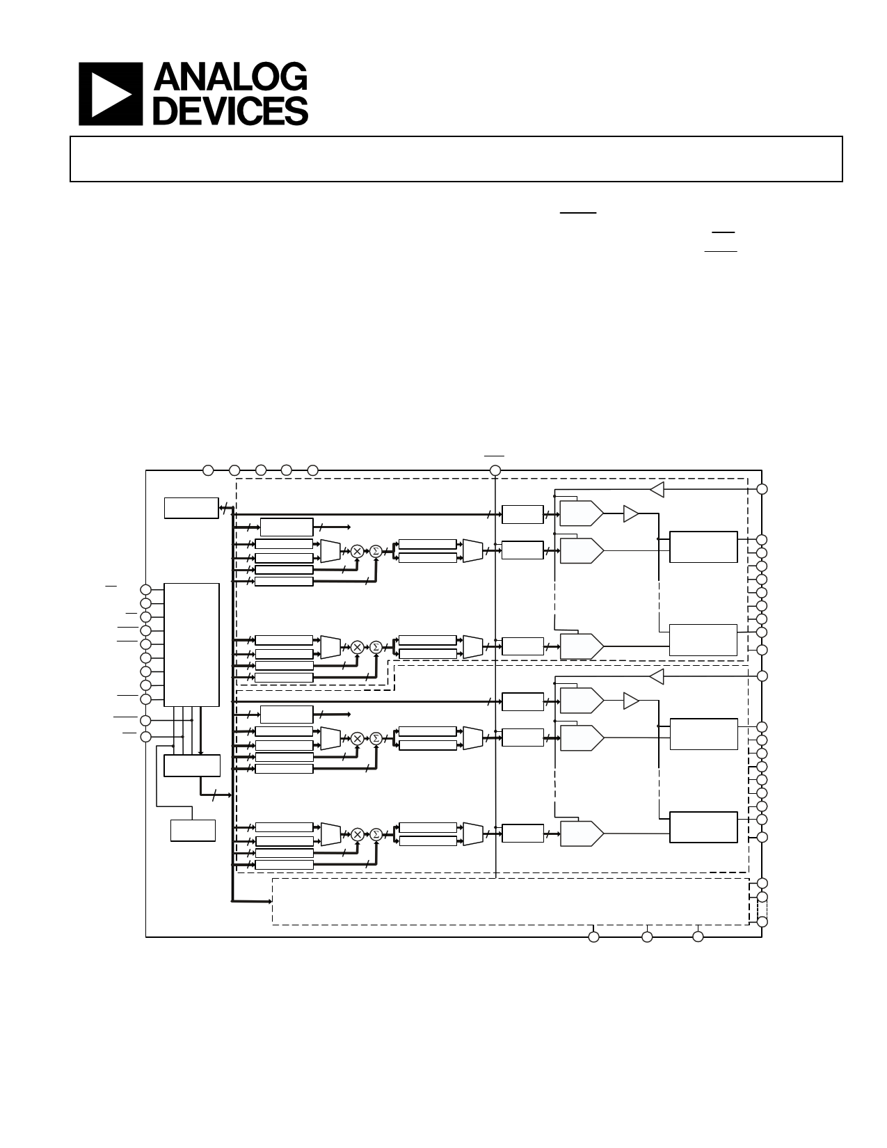
FUNCTIONAL BLOCK DIAGRAM
DVCC VDD VSS AGND DNGD
LDAC
SPI/LVDS
SYNC
SDI
SCLK
SYNC
SDI
SCLK
SDO
BUSY
RESET
CLR
CONTROL
REGISTER
SERIAL
INTERFACE
14
8
14
14
14
14
14
14
14
14
A/B SELECT 8
REGISTER
TO
MUX 2's
X1A REGISTER
X1B REGISTER
M REGISTER
C REGISTER
······
X1A REGISTER
14
MUX
1
14
14
14
······ ······
MUX 14
······
14
X1B REGISTER
M REGISTER
C REGISTER
1
14
14
X2A REGISTER
X2B REGISTER
·
·
·
·
·
·
X2A REGISTER
X2B REGISTER
14
MUX 14
2
·
·
·
·
·
·
MUX 14
2
OFS0 14
REGISTER
DAC 0 14
REGISTER
·
·
·
·
·
·
DAC 7 14
REGISTER
OFFSET
DAC 0
DAC 0
····
··
DAC 7
STATE
MACHINE
14
POWER-ON
RESET
AD5371
14 OFS1 14 OFFSET
8 A/B SELECT 8
TO
REGISTER
DAC 1
REGISTER
MUX 2's
14 X1A REGISTER
14 X1B REGISTER
14
M REGISTER
14 C REGISTER
······
14 X1A REGISTER
14 X1B REGISTER
14
M REGISTER
14 C REGISTER
14
MUX
1
14
14
14
······ ······
MUX 14
1
14
······
14
14
X2A REGISTER
X2B REGISTER
·
·
·
·
·
·
X2A REGISTER
X2B REGISTER
MUX 14
2
·
·
·
·
·
·
MUX 14
2
DAC 0 14
REGISTER
·
·
·
·
·
·
DAC 7 14
REGISTER
DAC 0
·
···
··
DAC 7
GROUPS 2 TO 4
SAME AS GROUP 1
BUFFER
GROUP 0
BUFFER
OUTPUT BUFFER
AND POWER
DOWN CONTROL
·
···
··
OUTPUT BUFFER
AND POWER
DOWN CONTROL
GROUP 1
BUFFER
OUTPUT BUFFER
AND POWER
DOWN CONTROL
··
····
OUTPUT BUFFER
AND POWER
DOWN CONTROL
VREF2 SUPPLIES
GROUPS 2 TO 4
537 1-0 001
AD5371—Protected by U.S. Patent No. 5,969,657; other patents pending
Figure 1.
SIGGND2
SIGGND3 SIGGND4
VREF0
VOUT0
VOUT1
VOUT2
VOUT3
VOUT4
VOUT5
VOUT6
VOUT7
SIGGND0
VREF1
VOUT8
VOUT9
VOUT10
VOUT11
VOUT12
VOUT13
VOUT14
VOUT15
SIGGND1
VREF2
VOUT16
TO
VOUT39
Rev. PrF
Information furnished by Analog Devices is believed to be accurate and reliable.
However, no responsibility is assumed by Analog Devices for its use, nor for any
infringements of patents or other rights of third parties that may result from its use.
Specifications subject to change without notice. No license is granted by implication
or otherwise under any patent or patent rights of Analog Devices. Trademarks and
registered trademarks are the property of their respective companies.
One Technology Way, P.O. Box 9106, Norwood, MA 02062-9106, U.S.A.
Tel: 781.329.4700
www.analog.com
Fax: 781.326.8703 © 2006 Analog Devices, Inc. All rights reserved.
1 page 
Preliminary Technical Data
AD5371
Parameter
LVDS INTERFACE – Reduced Range Link
Digital Inputs2
Input Voltage Range
Input Differential Threshold
External Termination Resistance
Differential Input Voltage
POWER REQUIREMENTS
DVCC
VDD
VSS
Power Supply Sensitivity2
∆ Full Scale/∆ VDD
∆ Full Scale/∆ VSS
∆ Full Scale/∆ VCC
DICC
IDD
ISS
Power Dissipation
Power Dissipation Unloaded (P)
Junction Temperature3
B Version1
875/1575
--0.1/0.1
80/120
100
132
100
2.3/5.5
8/16.5
−4.5/−16.5
−75
−75
−90
2
14
14
250
130
Unit Test Conditions/Comments2
mV min/max
V min/max
Ω min/max
Ω typ
Ω max
mV min
V min/max
V min/max
V min/max
dB typ
dB typ
dB typ
mA max
mA max
mA max
mW
°C max
VCC = 5.5 V, VIH = VCC, VIL = GND.
Outputs unloaded.
Outputs unloaded.
VSS = -5.5 V, VDD = +9.5 V, DVCC = 2.5 V
TJ = TA + PTOTAL × θJ.
1 Temperature range for B Version: -40°C to +85°C. Typical specifications are at 25°C.
2 Guaranteed by design and characterization, not production tested.
3 Where θJ represents the package thermal impedance.
AC CHARACTERISTICS
DVCC = 2.5; VDD = 15 V; VSS = −15 V; VREF = 3 V; AGND = DGND = SIGGND = 0 V; CL = 200 pF to GND; RL = 10 kΩ to GND;
Gain (m), Offset (c) and DAC Offset registers at default values; all specifications TMIN to TMAX, unless otherwise noted.
Table 3. AC Characteristics
Parameter
DYNAMIC PERFORMANCE
Output Voltage Settling Time
Slew Rate
Digital-to-Analog Glitch Energy
Glitch Impulse Peak Amplitude
Channel-to-Channel Isolation
DAC-to-DAC Crosstalk
Digital Crosstalk
Digital Feedthrough
Output Noise Spectral Density @ 10 kHz
b Version1 Unit
Test Conditions/Comments
TBD µs typ
Full-scale change
30 µs max
1 V/µs typ
20 nV-s typ
10 mV max
100 dB typ VREF(+) = 2 V p-p, 1 kHz.
40
nV-s typ
Between DACs inside a group.
10
nV-s typ
Between DACs from different groups.
0.1 nV-s typ
1
nV-s typ
Effect of input bus activity on DAC output under test.
250 nV/(Hz)1/2 typ VREF = 0 V.
1 Guaranteed by design and characterization, not production tested.
Rev. PrF | Page 5 of 25
5 Page 
Preliminary Technical Data
AD5371
Table 5. Pin Function Descriptions
Pin Function
DVCC Logic Power Supply; 2.5 V to 5.5 V. These pins should be decoupled with 0.1 µF ceramic capacitors and 10 µF
capacitors.
VSS Negative Analog Power Supply; −4.5 V to −16.5 V for specified performance. These pins should be decoupled with 0.1
µF ceramic capacitors and 10 µF capacitors.
VDD Positive Analog Power Supply; +8 V to +16.5 V for specified performance. These pins should be decoupled with 0.1 µF
ceramic capacitors and 10 µF capacitors.
AGND
Ground for All Analog Circuitry. All AGND pins should be connected to the AGND plane.
DGND
Ground for All Digital Circuitry. All DGND pins should be connected to the DGND plane.
VREF0
Reference Input for DACs 0 to 7. This reference voltage is referred to AGND.
VREF1
Reference Input for DACs 8 to 15. reference This voltage is referred to AGND.
VREF2
VOUT0 to VOUT39
Reference Input for DACs 16 to 39. This reference voltage is referred to AGND.
DAC Outputs. Buffered analog outputs for each of the 40 DAC channels. Each analog output is capable of driving an
output load of 10 kΩ to ground. Typical output impedance of these amplifiers is 0.5 Ω.
SYNC
Active Low or Differential SYNC Input (Complement) for SPI or LVDS Interface. This is the frame synchronization signal
for the SPI or LVDS serial interface. See SPI and LVDS timing diagrams and descriptions for more details.
SCLK
Serial Clock Input for SPI or LVDS Interface. See SPI and LVDS timing diagrams and descriptions for more details.
SDI Serial Data Input for SPI or LVDS Interface. See SPI and LVDS timing diagrams and descriptions for more details.
SDO Serial Data Output for SPI Interface. CMOS output. SDO can be used for readback. Data is clocked out on SDO on the
rising edge of SCLK and is valid on the falling edge of SCLK.
SYNC
Differential SYNC Input for LVDS Interface . This is the frame synchronization signal for the LVDS serial interface. See
LVDS timing diagram and description for more details.
SCLK
Differential Serial Clock Input (Complement) for LVDS Interface. See LVDS timing diagrams and descriptions for more
details.
SDI Differential Serial Data Input (Complement) for LVDS Interface. See LVDS timing diagrams and descriptions for more
details.
CLR Asynchronous Clear Input (level sensitive, active low). See the Clear Function section for more information
SPI/LVDS
Selects between SPI (low) or LVDS (high) serial interface.
LDAC
Load DAC Logic Input (active low). See the BUSY AND LDAC FUNCTIONS section for more information
BUSY
Digital Input/Open-Drain Output. BUSY is open-drain when an output. See the BUSY AND LDAC FUNCTIONS section
for more information
RESET
Asynchronous Digital Reset Input.
SIGGND0
Reference Ground for DACs 0 to 7. VOUT0 to VOUT7 are referenced to this voltage.
SIGGND1
Reference Ground for DACs 8 to 15. VOUT8 to VOUT15 are referenced to this voltage.
SIGGND1
Reference Ground for DACs 16 to 23. VOUT16 to VOUT23 are referenced to this voltage.
SIGGND3
Reference Ground for DACs 24 and 31. VOUT24 to VOUT31 are referenced to this voltage.
SIGGND4
Reference Ground for DACs 32 to 39. VOUT32 to VOUT39 are referenced to this voltage.
TESTI
Test Input Pin. This pin should be connected to DGND
TESTO
Test Output Pin. This pin should be left unconnected
Rev. PrF | Page 11 of 25
11 Page | ||
| Páginas | Total 25 Páginas | |
| PDF Descargar | [ Datasheet AD5371.PDF ] | |
Hoja de datos destacado
| Número de pieza | Descripción | Fabricantes |
| AD537 | Integrated Circuit Voltage-to-Frequency Converter | Analog Devices |
| AD5370 | Voltage-Output DACs | Analog Devices |
| AD5371 | Voltage-Output DAC | Analog Devices |
| AD5372 | (AD5372 / AD5373) Voltage-Output DACs | Analog Devices |
| Número de pieza | Descripción | Fabricantes |
| SLA6805M | High Voltage 3 phase Motor Driver IC. |
Sanken |
| SDC1742 | 12- and 14-Bit Hybrid Synchro / Resolver-to-Digital Converters. |
Analog Devices |
|
DataSheet.es es una pagina web que funciona como un repositorio de manuales o hoja de datos de muchos de los productos más populares, |
| DataSheet.es | 2020 | Privacy Policy | Contacto | Buscar |