|
|
PDF NB2669A Data sheet ( Hoja de datos )
| Número de pieza | NB2669A | |
| Descripción | Reduced EMI Clock Synthesizer | |
| Fabricantes | ON Semiconductor | |
| Logotipo | ||
Hay una vista previa y un enlace de descarga de NB2669A (archivo pdf) en la parte inferior de esta página. Total 8 Páginas | ||
|
No Preview Available !
www.DataSheet4U.com
NB2669A
Low Power, Reduced EMI
Clock Synthesizer
The NB2669A is a versatile spread spectrum frequency modulator
designed specifically for a wide range of clock frequencies. The
NB2669A reduces ElectroMagnetic Interference (EMI) at the clock
source, allowing system wide reduction of EMI of all clock dependent
signals. The NB2669A allows significant system cost savings by
reducing the number of circuit board layers, ferrite beads and
shielding that are traditionally required to pass EMI regulations.
The NB2669A uses the most efficient and optimized modulation
profile approved by the FCC and is implemented by using a
proprietary all digital method.
The NB2669A modulates the output of a single PLL in order to
“spread” the bandwidth of a synthesized clock, and more importantly,
decreases the peak amplitudes of its harmonics. This results in
significantly lower system EMI compared to the typical narrow band
signal produced by oscillators and most frequency generators.
Lowering EMI by increasing a signal’s bandwidth is called ‘spread
spectrum clock generation’.
The NB2669A is targeted towards all portable devices with very
low power requirements like MP3 players and digital still cameras.
Features
• Generates an EMI Optimized Clocking Signal at the Output
• Integrated Loop Filter Components
• Operates with a 3.3 V / 2.5 V Supply
• Operating Current less than 4.0 mA
• Low Power CMOS Design
• Input Frequency Range: 6.0 MHz to 12 MHz for 2.5 V
Input Frequency Range: 6.0 MHz to 13 MHz for 3.3 V
• Generates a 1X Low EMI Spread Spectrum clock of the Input
Frequency
• Frequency Deviation "1% @ 10 MHz
• Available in TSOP−6 Package (TSOT−23−6)
• Pb−Free Package is Available
http://onsemi.com
MARKING
DIAGRAM*
6
1
TSOP−6
(TSOT−23−6)
SN SUFFIX
CASE 318G
E02AYWG
G
1
E02 = Specific Device Code
A = Assembly Location
Y = Year
W = Work Week
G = Pb−Free Package
(Note: Microdot may be in either location)
*For additional marking information, refer to
Application Note AND8002/D.
ORDERING INFORMATION
See detailed ordering and shipping information in the package
dimensions section on page 7 of this data sheet.
© Semiconductor Components Industries, LLC, 2006
December, 2006 − Rev. 3
1
Publication Order Number:
NB2669A/D
1 page 
NB2669A
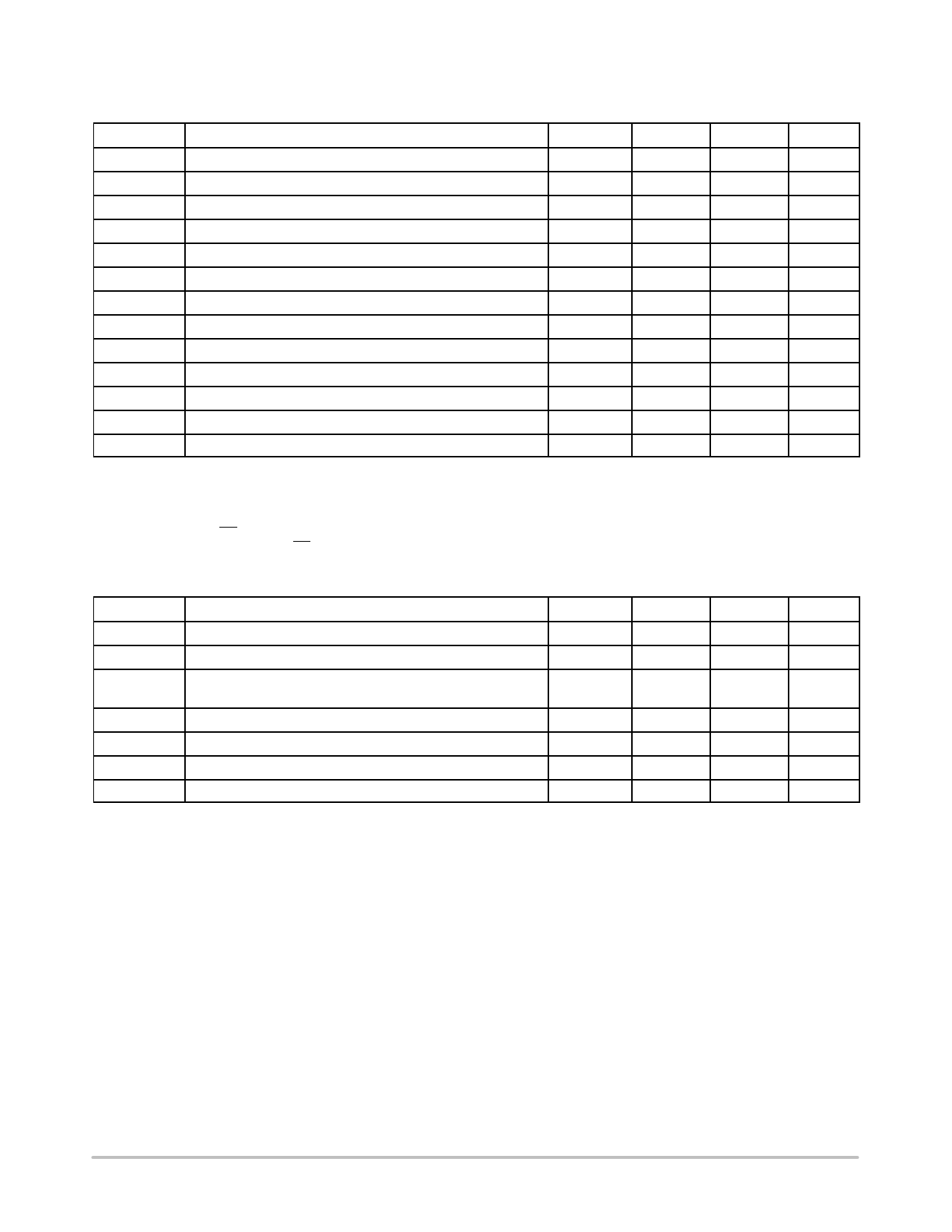
Table 6. DC ELECTRICAL CHARACTERISTICS FOR 3.3 V SUPPLY (Test Conditions: All parameters are measured at room
temperature 25°C)
Symbol
Description
Min Typ Max Unit
VIL Input LOW Voltage
GND − 0.3
0.8 V
VIH Input HIGH Voltage
2.0
VDD + 0.3
V
IIL Input LOW Current
−35 mA
IIH Input HIGH Current
35 mA
IXOL XOUT Output LOW Current (@ 0.4 V, VDD = 3.3 V)
3.0 mA
IXOH
XOUT Output HIGH Current (@ 2.5 V, VDD = 3.3 V)
3.0 mA
VOL Output LOW Voltage (VDD = 3.3 V, IOL = 8.0 mA)
0.4 V
VOH Output HIGH Voltage (VDD = 3.3 V, IOH = 8.0 mA)
2.5
V
IDD Static Supply Current (Note 4)
10 mA
ICC Dynamic Supply Current (3.3 V, 10 MHz, and No Load)
2.5 mA
VDD Operating Voltage
2.7 3.3 3.6 V
tON PLL first locked cycle time (Note 5)
5.0 mS
ZOUT
Clock Output Impedance
45 W
NOTE: Device will meet the specifications after thermal equilibrium has been established when mounted in a test socket or printed circuit
board with maintained transverse airflow greater than 500 lfpm. Electrical parameters are guaranteed only over the declared
operating temperature range. Functional operation of the device exceeding these conditions is not implied. Device specification limit
values are applied individually under normal operating conditions and not valid simultaneously.
4. XIN/CLKIN pin and PD pin are pulled low.
5. VDD and CLKIN input are stable, PD pin is made high from low.
Table 7. AC ELECTRICAL CHARACTERISTICS FOR 3.3 V SUPPLY
Symbol
Description
Min Typ Max Unit
CLKIN
Input Frequency
6 13 MHz
ModOUT
Output Frequency
6 13 MHz
fd Frequency Deviation
Input Frequency = 6.0 MHz
Input Frequency = 13 MHz
±1.48
±0.74
%
tLH (Note 6) Output Rise Time (measured at 0.8 V to 2.0 V)
0.5 1.3 1.5 ns
tHL (Note 6) Output Fall Time (measured at 2.0 V to 0.8 V)
0.4 0.9 1.1 ns
tJC Jitter (Cycle−to−Cycle)
200 ps
tD Output Duty Cycle
45 50 55 %
NOTE: Device will meet the specifications after thermal equilibrium has been established when mounted in a test socket or printed circuit
board with maintained transverse airflow greater than 500 lfpm. Electrical parameters are guaranteed only over the declared
operating temperature range. Functional operation of the device exceeding these conditions is not implied. Device specification limit
values are applied individually under normal operating conditions and not valid simultaneously.
6. tLH and tHL are measured at capacitive load of 15 pF.
http://onsemi.com
5
5 Page | ||
| Páginas | Total 8 Páginas | |
| PDF Descargar | [ Datasheet NB2669A.PDF ] | |
Hoja de datos destacado
| Número de pieza | Descripción | Fabricantes |
| NB2669A | Reduced EMI Clock Synthesizer | ON Semiconductor |
| Número de pieza | Descripción | Fabricantes |
| SLA6805M | High Voltage 3 phase Motor Driver IC. |
Sanken |
| SDC1742 | 12- and 14-Bit Hybrid Synchro / Resolver-to-Digital Converters. |
Analog Devices |
|
DataSheet.es es una pagina web que funciona como un repositorio de manuales o hoja de datos de muchos de los productos más populares, |
| DataSheet.es | 2020 | Privacy Policy | Contacto | Buscar |
