|
|
|
PDF ADG888 Data sheet ( Hoja de datos )
| Número de pieza | ADG888 | |
| Descripción | Dual DPDT Switch | |
| Fabricantes | Analog Devices | |
| Logotipo | ||
Hay una vista previa y un enlace de descarga de ADG888 (archivo pdf) en la parte inferior de esta página. Total 16 Páginas | ||
|
No Preview Available !
www.DataSheet4U.com
0.4 Ω CMOS, Dual DPDT Switch
in WLCSP/LFCSP/TSSOP Packages
ADG888
FEATURES
1.8 V to 5.5 V operation
Ultralow on resistance
0.4 Ω typical
0.6 Ω maximum at 5 V supply
Excellent audio performance, ultralow distortion
0.07 Ω typical
0.14 Ω maximum RON flatness
High current carrying capability
400 mA continuous
600 mA peak current at 5 V
Automotive temperature range: −40°C to +125°C
Rail-to-rail switching operation
Typical power consumption (<0.1 μW)
APPLICATIONS
Cellular phones
PDAs
MP3 players
Power routing
Battery-powered systems
PCMCIA cards
Modems
Audio and video signal routing
Communication systems
Data switching
GENERAL DESCRIPTION
The ADG888 is a low voltage, dual DPDT (double-pole,
double-throw) CMOS device optimized for high performance
audio switching. With its low power and small physical size, it is
ideal for portable devices.
This device offers ultralow on resistance of less than 0.8 Ω over
the full temperature range, making it an ideal solution for
applications requiring minimal distortion through the switch.
The ADG888 also has the capability of carrying large amounts
of current, typically 400 mA at 5 V operation.
When on, each switch conducts equally well in both directions
and has an input signal range that extends to the supplies. The
ADG888 exhibits break-before-make switching action.
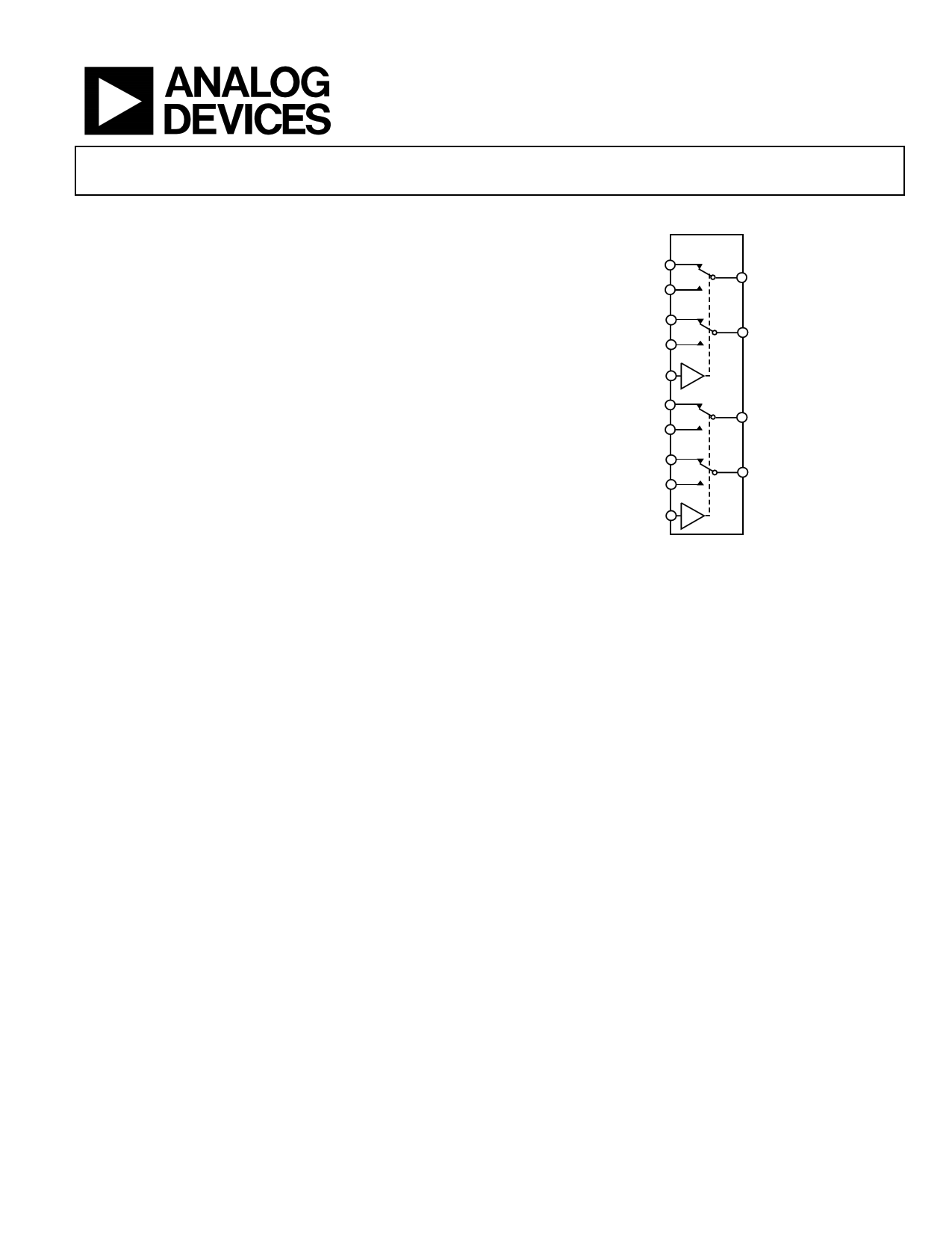
FUNCTIONAL BLOCK DIAGRAM
ADG888
S1A
S1B
D1
S2A
S2B
D2
IN1
S3A
S3B
S4A
S4B
D3
D4
IN2
SWITCHES SHOWN
FOR A LOGIC 1 INPUT
Figure 1.
The ADG888 is available in a 16-ball WLCSP, 16-lead LFCSP,
and a 16-lead TSSOP. These packages make the ADG888 the
ideal solution for space-constrained applications.
PRODUCT HIGHLIGHTS
1. <0.6 Ω over full temperature range of −40°C to +125°C.
2. High current handling capability (400 mA continuous
current at 5 V).
3. Low THD + N (0.008% typical).
4. Tiny 16-ball WLCSP, 16-lead LFCSP, and 16-lead TSSOP.
Rev. A
Information furnished by Analog Devices is believed to be accurate and reliable. However, no
responsibility is assumed by Analog Devices for its use, nor for any infringements of patents or other
rights of third parties that may result from its use. Specifications subject to change without notice. No
license is granted by implication or otherwise under any patent or patent rights of Analog Devices.
Trademarksandregisteredtrademarksarethepropertyoftheirrespectiveowners.
One Technology Way, P.O. Box 9106, Norwood, MA 02062-9106, U.S.A.
Tel: 781.329.4700
www.analog.com
Fax: 781.461.3113
©2006 Analog Devices, Inc. All rights reserved.
1 page 
ABSOLUTE MAXIMUM RATINGS
TA = 25°C, unless otherwise noted.
Table 3.
Parameter
VDD to GND
Analog Inputs, Digital Inputs1
Peak Current, S or D
5 V operation
Continuous Current, S or D
5 V operation
Operating Temperature Range
Automotive (Y Version)
TSSOP and LFCSP packages
Industrial (B version)
WLCSP package
Storage Temperature Range
Junction Temperature
16-Lead TSSOP Package
θJA Thermal Impedance
(4-Layer Board)
θJC Thermal Impedance
16-Lead WLCSP Package
θJA Thermal Impedance
(4-Layer Board)
16-Lead LFCSP Package
θJA Thermal Impedance
(4-Layer Board)
Reflow Soldering (Pb-Free)
Peak Temperature
Time at Peak Temperature
Rating
−0.3 V to +6 V
−0.3 V to VDD + 0.3 V or 30 mA,
whichever occurs first
600 mA (pulsed at 1 ms,
10% duty cycle max)
400 mA
−40°C to +125°C
−40°C to +85°C
−65°C to +150°C
150°C
112°C/W
27.6°C/W
130°C/W
30.4°C/W
260(+0/−5)°C
10 sec to 40 sec
1 Overvoltages at IN, S, or D are clamped by internal diodes. Limit current to
the maximum ratings given.
ADG888
Stresses above those listed under Absolute Maximum Ratings
may cause permanent damage to the device. This is a stress
rating only; functional operation of the device at these or any
other conditions above those indicated in the operational
section of this specification is not implied. Exposure to absolute
maximum rating conditions for extended periods may affect
device reliability.
Only one absolute maximum rating can be applied at any one
time.
ESD CAUTION
Rev. A | Page 5 of 16
5 Page 
TERMINOLOGY
IDD
Positive supply current.
VD (VS)
Analog voltage on Terminal D and Terminal S.
RON
Ohmic resistance between Terminal D and Terminal S.
RFLAT (ON)
Flatness is defined as the difference between the maximum and
minimum value of on resistance as measured.
ΔRON
On resistance match between any two channels.
IS (OFF)
Source leakage current with the switch off.
ID, IS (ON)
Channel leakage current with the switch on.
VINL
Maximum input voltage for Logic 0.
VINH
Minimum input voltage for Logic 1.
IINL (IINH)
Input current of the digital input.
CS (OFF)
Off switch source capacitance. Measured with reference to
ground.
CD, CS (ON)
On switch capacitance. Measured with reference to ground.
CIN
Digital input capacitance.
tON
Delay time between the 50% and the 90% points of the digital
input and switch on condition.
ADG888
tOFF
Delay time between the 50% and the 90% points of the digital
input and switch off condition.
tBBM
On or off time measured between the 80% points of both
switches when switching from one to another.
Charge Injection
A measure of the glitch impulse transferred from the digital
input to the analog output during on-off switching.
Off Isolation
A measure of unwanted signal coupling through an off switch.
Crosstalk
A measure of unwanted signal that is coupled through from one
channel to another as a result of parasitic capacitance. This is
specified for two conditions:
• Adjacent channel, that is, S1A to S2A, S1B to S2B, S3A to
S4A, or S3B to S4B.
• Adjacent switch, that is, S1A to S1B, S2A to S2B, S3A to
S3B, or S4A to S4B.
−3 dB Bandwidth
The frequency at which the output is attenuated by 3 dB.
On Response
The frequency response of the on switch.
Insertion Loss
The loss due to the on resistance of the switch.
THD + N
The ratio of the harmonic amplitudes plus signal noise to the
fundamental.
Rev. A | Page 11 of 16
11 Page | ||
| Páginas | Total 16 Páginas | |
| PDF Descargar | [ Datasheet ADG888.PDF ] | |
Hoja de datos destacado
| Número de pieza | Descripción | Fabricantes |
| ADG884 | DUAL 2:1 MUX/SPDT AUDIO SWITCH | Analog Devices |
| ADG888 | Dual DPDT Switch | Analog Devices |
| Número de pieza | Descripción | Fabricantes |
| SLA6805M | High Voltage 3 phase Motor Driver IC. |
Sanken |
| SDC1742 | 12- and 14-Bit Hybrid Synchro / Resolver-to-Digital Converters. |
Analog Devices |
|
DataSheet.es es una pagina web que funciona como un repositorio de manuales o hoja de datos de muchos de los productos más populares, |
| DataSheet.es | 2020 | Privacy Policy | Contacto | Buscar |