|
|
|
PDF ADG841 Data sheet ( Hoja de datos )
| Número de pieza | ADG841 | |
| Descripción | (ADG841 / ADG842) 0.28 OHM CMOS 1.65 V to 3.6 V Single SPST Switches | |
| Fabricantes | Analog Devices | |
| Logotipo | ||
Hay una vista previa y un enlace de descarga de ADG841 (archivo pdf) en la parte inferior de esta página. Total 16 Páginas | ||
|
No Preview Available !
www.DataSheet4U.com
FEATURES
Ultralow on resistance
0.28 Ω typical
0.48 Ω max at 125°C
Excellent audio performance, ultralow distortion
0.025 Ω typical
0.052 Ω max RON flatness
1.65 V to 3.6 V single supply
High current carrying capability
300 mA continuous current
500 mA peak current
Automotive temperature range: –40°C to +125°C
Rail-to-rail operation
Typical power consumption (<0.01 µW)
APPLICATIONS
Handsets
PDAs
MP3 players
Power routing
Battery-powered systems
Communication systems
Modems
PCMCIA cards
GENERAL DESCRIPTION
The ADG841 and ADG842 are low voltage CMOS devices
containing a single-pole, single-throw (SPST) switch. The
ADG841 is closed for a Logic 1 input and the ADG842 is open
for a Logic 1 input. The devices offer ultralow on resistance of
less than 0.48 Ω over the full temperature range. The ADG841/
ADG842 are fully specified for 3.3 V, 2.5 V, and 1.8 V supply
operation.
Each switch conducts equally well in both directions when on,
and has an input signal range that extends to the supplies. The
ADG841/ADG842 exhibit break-before-make switching action.
The ADG841/ADG842 are available in a 6-lead SC70 package.
0.28 Ω CMOS 1.65 V to 3.6 V
Single SPST Switches in SC70
ADG841/ADG842
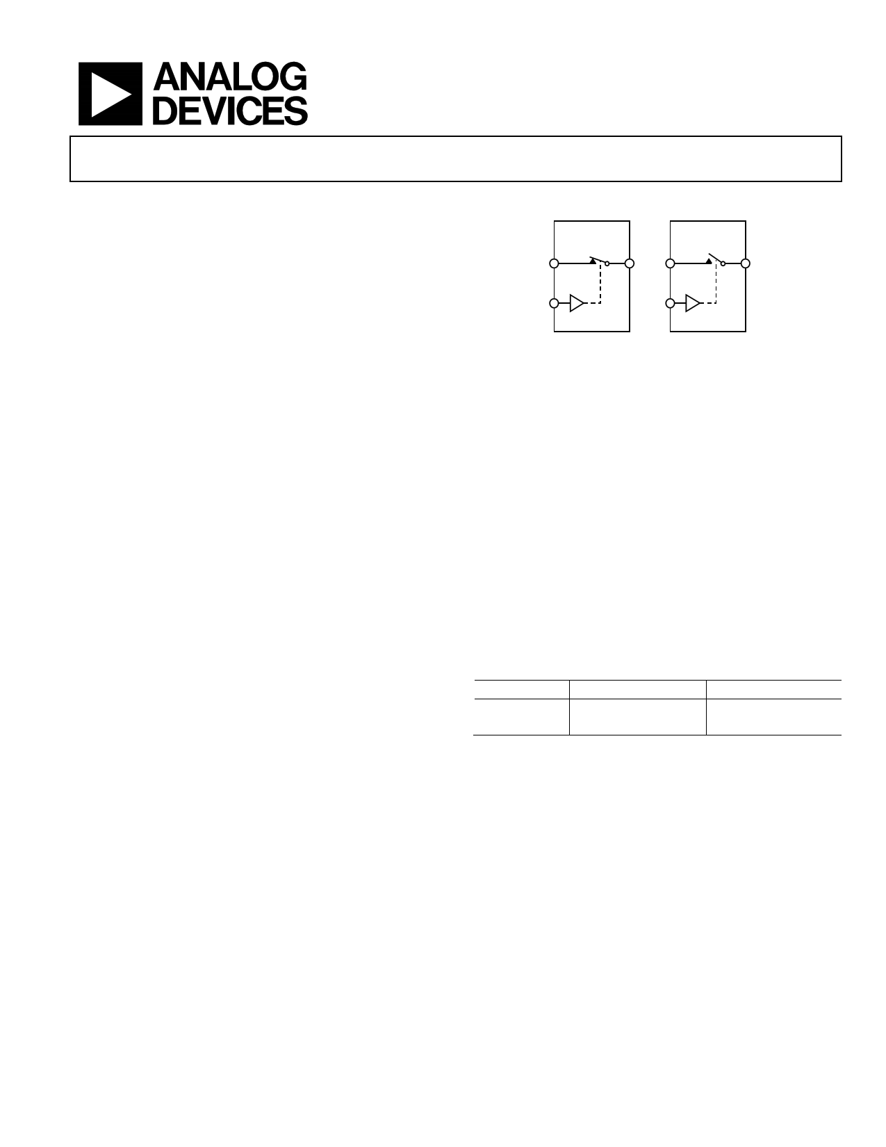
FUNCTIONAL BLOCK DIAGRAM
ADG841
ADG842
S DS D
IN IN
SWITCHES SHOWN
FOR A LOGIC 1 INPUT
Figure 1.
PRODUCT HIGHLIGHTS
1. <0.48 Ω over full temperature range of –40°C to +125°C.
2. Compatible with 1.8 V CMOS logic.
3. High current handling capability (300 mA continuous
current at 3.3 V).
4. Low THD + N (0.02% typ).
5. Tiny SC70 package.
Table 1. ADG841/ADG842 Truth Table
Logic (IN)
ADG841
ADG842
0 Off
On
1 On
Off
Rev. 0
Information furnished by Analog Devices is believed to be accurate and reliable.
However, no responsibility is assumed by Analog Devices for its use, nor any
infringements of patents or other rights of third parties that may result from its use.
Specifications subject to change without notice. No license is granted by implication
or otherwise under any patent or patent rights of Analog Devices. Trademarks and
registered trademarks are the property of their respective owners.
One Technology Way, P.O. Box 9106, Norwood, MA 02062-9106, U.S.A.
Tel: 781.329.4700
www.analog.com
Fax: 781.461.3113 © 2005 Analog Devices, Inc. All rights reserved.
1 page 
ADG841/ADG842
SPECIFICATIONS—1.65 V TO 1.951
VDD = 1.65 V to1.95 V, GND = 0 V, unless otherwise noted.
Table 4.
Parameter
ANALOG SWITCH
Analog Signal Range
On Resistance (RON)
On Resistance Flatness (RFLAT (ON))
LEAKAGE CURRENTS
Source Off Leakage IS (OFF)
Channel On Leakage ID, IS (ON)
DIGITAL INPUTS
Input High Voltage, VINH
Input Low Voltage, VINL
Input Current, IINL or IINH
+25°C
−40°C
to +85°C
0.37
0.4 0.84
0.6 1.8
0.17
±0.2
±0.2
0.005
Digital Input Capacitance, CIN
DYNAMIC CHARACTERISTICS2
tON
tOFF
Charge Injection
Off Isolation
Total Harmonic Distortion (THD + N)
Insertion Loss
–3 dB Bandwidth
CS (OFF)
CD (OFF)
CD, CS (ON)
POWER REQUIREMENTS
IDD
4
19
26
8
9.5
100
−54
0.14
−0.02
21
178
178
238
0.003
1 Temperature range −40°C to +125°C.
2 Guaranteed by design; not subject to production test.
28
9.8
1
−40°C
to +125°C Unit
0 V to VDD
0.84
1.8
V
Ω typ
Ω max
Ω max
Ω typ
nA typ
nA typ
0.65 VDD
0.35 VDD
±0.1
V min
V max
µA typ
µA max
pF typ
ns typ
30 ns max
ns typ
10 ns max
pC typ
dB typ
%
dB typ
MHz typ
pF typ
pF typ
pF typ
µA typ
4 µA max
Test Conditions/Comments
VDD = 1.8 V, VS = 0 V to VDD, IDS = −100 mA
Figure 18
VDD = 1.65 V, VS = 0 V to VDD, IDS = −100 mA
VDD = 1.65 V, VS = 0 V to VDD, IDS = −100 mA
VDD = 1.95 V
VS = 0.6 V/1.65 V, VD = 1.65 V/0.6 V; Figure 19
VS = VD = 0.6 V or 1.65 V; Figure 20
VIN = VINL or VINH
RL = 50 Ω, CL = 35 pF
VS = 1.5 V; Figure 21
RL = 50 Ω, CL = 35 pF
VS = 1.5 V; Figure 21
VS = 1 V, RS = 0 V, CL = 1 nF; Figure 22
RL = 50 Ω, CL = 5 pF, f = 100 kHz; Figure 23
RL = 32 Ω, f = 20 Hz to 20 kHz, VS = 1.2 V p-p
RL = 50 Ω, CL = 5 pF; Figure 24
RL = 50 Ω, CL = 5 pF; Figure 24
VDD = 1.95 V
Digital inputs = 0 V or 1.95 V
Rev. 0 | Page 5 of 16
5 Page 
TERMINOLOGY
IDD
Positive supply current.
VD (VS)
Analog voltage on Terminals D and S.
RON
Ohmic resistance between D and S.
RFLAT (ON)
Flatness is the difference between the maximum and minimum
value of on resistance as measured over the specified analog
signal range.
IS (OFF)
Source leakage current with the switch off.
ID (OFF)
Drain leakage current with the switch off.
ID, IS (ON)
Channel leakage current with the switch on.
VINL
Maximum input voltage for Logic 0.
VINH
Minimum input voltage for Logic 1.
IINL (IINH)
Input current of the digital input.
CS (OFF)
Off switch source capacitance. Measured with reference to
ground.
CD (OFF)
Off switch drain capacitance. Measured with reference to
ground.
ADG841/ADG842
CD, CS (ON)
On switch capacitance. Measured with reference to ground.
CIN
Digital input capacitance.
tON
Delay time between the 50% and the 90% points of the digital
input and switch on condition.
tOFF
Delay time between the 50% and the 90% points of the digital
input and switch off condition.
Charge Injection
A measure of the glitch impulse transferred from the digital
input to the analog output during on-off switching.
Off Isolation
A measure of unwanted signal coupling through an off switch.
−3 dB Bandwidth
The frequency at which the output is attenuated by 3 dB.
On Response
The frequency response of the on switch.
Insertion Loss
The loss due to the on resistance of the switch.
THD + N
The ratio of the harmonics amplitude plus noise of a signal to
the fundamental.
PSRR
Power Supply Rejection Ratio. This is a measure of the coupling
of unwanted ac signals on the power supply to the switch output
when the supply is not decoupled.
Rev. 0 | Page 11 of 16
11 Page | ||
| Páginas | Total 16 Páginas | |
| PDF Descargar | [ Datasheet ADG841.PDF ] | |
Hoja de datos destacado
| Número de pieza | Descripción | Fabricantes |
| ADG841 | (ADG841 / ADG842) 0.28 OHM CMOS 1.65 V to 3.6 V Single SPST Switches | Analog Devices |
| ADG842 | (ADG841 / ADG842) 0.28 OHM CMOS 1.65 V to 3.6 V Single SPST Switches | Analog Devices |
| ADG849 | 3 V/5 V CMOS 0.5 Ohm SPDT/2:1 Mux | Analog Devices |
| Número de pieza | Descripción | Fabricantes |
| SLA6805M | High Voltage 3 phase Motor Driver IC. |
Sanken |
| SDC1742 | 12- and 14-Bit Hybrid Synchro / Resolver-to-Digital Converters. |
Analog Devices |
|
DataSheet.es es una pagina web que funciona como un repositorio de manuales o hoja de datos de muchos de los productos más populares, |
| DataSheet.es | 2020 | Privacy Policy | Contacto | Buscar |