|
|
|
PDF ADF7020-1 Data sheet ( Hoja de datos )
| Número de pieza | ADF7020-1 | |
| Descripción | High Performance FSK/ASK Transceiver IC | |
| Fabricantes | Analog Devices | |
| Logotipo | ||
Hay una vista previa y un enlace de descarga de ADF7020-1 (archivo pdf) en la parte inferior de esta página. Total 48 Páginas | ||
|
No Preview Available !
www.DataSheet4U.com
FEATURES
Low power, low IF transceiver
Frequency bands
135 MHz to 650 MHz, direct output
80 MHz to 325 MHz, divide-by-2 mode
Data rates supported
0.15 kbps to 200 kbps, FSK
0.15 kbps to 64 kbps, ASK
2.3 V to 3.6 V power supply
Programmable output power
−20 dBm to +13 dBm in 63 steps
Receiver sensitivity
−119 dBm at 1 kbps, FSK, 315 MHz
−114 dBm at 9.6 kbps, FSK, 315 MHz
−111.8 dBm at 9.6 kbps, ASK, 315 MHz
Low power consumption
17.6 mA in receive mode
21 mA in transmit mode (10 dBm output)
High Performance
FSK/ASK Transceiver IC
ADF7020-1
On-chip VCO and fractional-N PLL
On-chip 7-bit ADC and temperature sensor
Fully automatic frequency control loop (AFC) compensates
for lower tolerance crystals
Digital RSSI
Integrated TRx switch
Leakage current <1 μA in power-down mode
APPLICATIONS
Low cost wireless data transfer
Wireless medical applications
Remote control/security systems
Wireless metering
Keyless entry
Home automation
Process and building control
RSET
CREG(1:4)
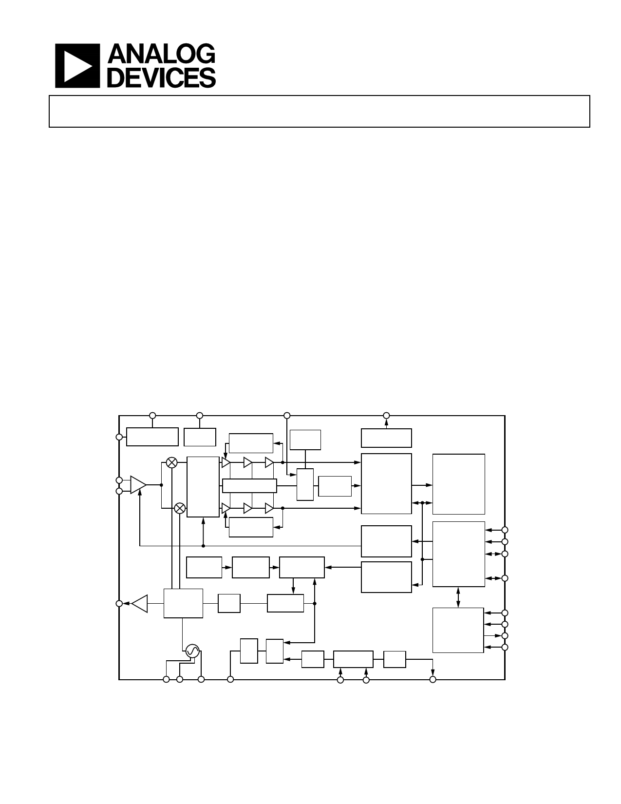
FUNCTIONAL BLOCK DIAGRAM
ADCIN
MUXOUT
RLNA
POLARIZATION LDO(1:4)
OFFSET
CORRECTION
TEMP
SENSOR
TEST MUX
RFIN
RFINB
RFOUT
LNA
GAIN
IF FILTER
RSSI
MUX 7-BIT ADC
FSK/ASK
DEMODULATOR
OFFSET
CORRECTION
AGC
CONTROL
FSK MOD
CONTROL
GAUSSIAN
FILTER
Σ-Δ
MODULATOR
AFC
CONTROL
DIVIDERS/
MUXING
DIV P
N/N+1
VCO
CP PFD
DIV R
RING OSC
CLK
DIV
DATA
SYNCHRONIZER
Tx/Rx
CONTROL
SERIAL
PORT
L1 L2 VCOIN CPOUT
OSC1 OSC2
Figure 1.
CLKOUT
CE
DATA CLK
DATA I/O
INT/LOCK
SLE
SDATA
SREAD
SCLK
Rev. 0
Information furnished by Analog Devices is believed to be accurate and reliable. However, no
responsibility is assumed by Analog Devices for its use, nor for any infringements of patents or other
rights of third parties that may result from its use. Specifications subject to change without notice. No
license is granted by implication or otherwise under any patent or patent rights of Analog Devices.
Trademarksandregisteredtrademarksarethepropertyoftheirrespectiveowners.
One Technology Way, P.O. Box 9106, Norwood, MA 02062-9106, U.S.A.
Tel: 781.329.4700
www.analog.com
Fax: 781.461.3113
© 2005 Analog Devices, Inc. All rights reserved.
1 page 
Parameter
RECEIVER PARAMETERS
FSK/GFSK Input Sensitivity
Sensitivity at 1 kbps
Sensitivity at 9.6 kbps
OOK Input Sensitivity
Sensitivity at 1 kbps
Sensitivity at 9.6 kbps
LNA and Mixer, Input IP37
Enhanced Linearity Mode
Low Current Mode
High Sensitivity Mode
Rx Spurious Emissions8
Min
AFC
Pull-In Range
Response Time
Accuracy
CHANNEL FILTERING
Adjacent Channel Rejection
(Offset = ±1 × IF Filter BW
Setting)
Second Adjacent Channel Rejection
(Offset = ±2 × IF Filter BW
Setting)
Third Adjacent Channel Rejection
(Offset = ±3 × IF Filter BW
Setting)
Image Channel Rejection
CO-CHANNEL REJECTION
Wideband Interference Rejection
BLOCKING
±1 MHz
±5 MHz
±10 MHz
±10 MHz (High Linearity Mode)
Saturation (Maximum Input Level)
LNA Input Impedance
RSSI
Range at Input
Linearity
Absolute Accuracy
Response Time
Typ Max
−119.2
−114.2
−118.2
−111.8
6.8
−3.2
−35
±50
48
1
27
50
55
35
−2
70
−57
−47
60
68
65
72
12
237 − j193
101.4 − j161.6
49.3 − j104.6
−100 to −36
±2
±3
150
ADF7020-1
Unit Test Conditions
dBm
dBm
dBm
dBm
At BER = 1E − 3, FRF = 315 MHz,
LNA and PA matched separately6
FDEV= 5 kHz, high sensitivity mode7
FDEV = 10 kHz, high sensitivity mode
At BER = 1E − 3, FRF = 315 MHz
High sensitivity mode
High sensitivity mode
dBm Pin = −20 dBm, 2 CW interferers,
dBm FRF = 315 MHz, F1 = FRF + 3 MHz,
dBm F2 = FRF + 6 MHz, maximum gain
dBm <1 GHz at antenna input
dBm >1 GHz at antenna input
kHz IF_BW = 200 kHz
Bits Modulation index = 0.875
kHz
dB IF filter BW settings = 100 kHz, 150 kHz,
200 kHz; desired signal 3 dB above the input
sensitivity level; CW interferer power level
dB increased until BER = 10−3; image channel
excluded
dB
dB
dB
dB
dB
dB
dB
dB
dBm
Ω
Ω
Ω
dBm
dB
dB
μs
Image at FRF − 400 kHz
Swept from 100 MHz to 2 GHz, measured as
channel rejection
Desired signal 3 dB above the input sensitivity
level, CW interferer power level increased
until BER = 10−2
FSK mode, BER = 10−3
FRF = 130 MHz, RFIN to GND
FRF = 310 MHz
FRF = 610 MHz
See the RSSI/AGC section
Rev. 0 | Page 5 of 48
5 Page 
PIN CONFIGURATION AND FUNCTION DESCRIPTIONS
ADF7020-1
VCOIN 1
CREG1 2
VDD1 3
RFOUT 4
RFGND 5
RFIN 6
RFINB 7
RLNA 8
VDD4 9
RSET 10
CREG4 11
GND4 12
PIN 1
INDICATOR
ADF7020-1
TOP VIEW
(Not to Scale)
36 CLKOUT
35 DATA CLK
34 DATA I/O
33 INT/LOCK
32 VDD2
31 CREG2
30 ADCIN
29 GND2
28 SCLK
27 SREAD
26 SDATA
25 SLE
Figure 6. Pin Configuration
Table 4. Pin Function Descriptions
Pin No. Mnemonic Description
1 VCOIN VCO Input Pin. The tuning voltage on this pin determines the output frequency of the voltage controlled
oscillator (VCO). The higher the tuning voltage, the higher the output frequency.
2 CREG1 Regulator Voltage for PA Block. A 100 nF in parallel with a 5.1 pF capacitor should be placed between this pin
and ground for regulator stability and noise rejection.
3 VDD1
Voltage Supply for PA Block. Decoupling capacitors of 0.1 μF and 10 pF should be placed as close as possible to
this pin. All VDD pins should be tied together.
4
RFOUT
PA Output Pin. The modulated signal is available at this pin. Output power levels are from −20 dBm to +13 dBm.
The output should be impedance matched to the desired load using suitable components. See the Transmitter
section.
5
RFGND
Ground for Output Stage of Transmitter. All GND pins should be tied together.
6 RFIN
LNA Input for Receiver Section. Input matching is required between the antenna and the differential LNA input
to ensure maximum power transfer. See the LNA/PA Matching section.
7 RFINB
Complementary LNA Input. See the LNA/PA Matching section.
8 RLNA
External Bias Resistor for LNA. Optimum resistor is 1.1 kΩ with 5% tolerance.
9 VDD4
Voltage Supply for LNA/MIXER Block. This pin should be decoupled to ground with a 10 nF capacitor.
10 RSET
External Resistor to Set Charge Pump Current and Some Internal Bias Currents. Use 3.6 kΩ with 5% tolerance.
11 CREG4
Regulator Voltage for LNA/MIXER Block. A 100 nF capacitor should be placed between this pin and GND for
regulator stability and noise rejection.
12 GND4
Ground for LNA/MIXER Block.
13 to 18 MIX/FILT
Signal Chain Test Pins. These pins are high impedance under normal conditions and should be left
unconnected.
19, 22 GND4
Ground for LNA/MIXER Block.
20, 21,
23
FILT/TEST_A Signal Chain Test Pins. These pins are high impedance under normal conditions and should be left
unconnected.
24 CE
Chip Enable. Bringing CE low puts the ADF7020-1 into complete power-down. Register values are lost when CE
is low, and the part must be reprogrammed once CE is brought high.
25 SLE
Load Enable, CMOS Input. When LE goes high, the data stored in the shift registers is loaded into one of the
four latches. A latch is selected using the control bits.
26 SDATA
Serial Data Input. The serial data is loaded MSB first, with the 2 LSBs as the control bits. This pin is a high
impedance CMOS input.
Rev. 0 | Page 11 of 48
11 Page | ||
| Páginas | Total 48 Páginas | |
| PDF Descargar | [ Datasheet ADF7020-1.PDF ] | |
Hoja de datos destacado
| Número de pieza | Descripción | Fabricantes |
| ADF7020-1 | High Performance FSK/ASK Transceiver IC | Analog Devices |
| Número de pieza | Descripción | Fabricantes |
| SLA6805M | High Voltage 3 phase Motor Driver IC. |
Sanken |
| SDC1742 | 12- and 14-Bit Hybrid Synchro / Resolver-to-Digital Converters. |
Analog Devices |
|
DataSheet.es es una pagina web que funciona como un repositorio de manuales o hoja de datos de muchos de los productos más populares, |
| DataSheet.es | 2020 | Privacy Policy | Contacto | Buscar |