|
|
|
PDF ADSP-21375 Data sheet ( Hoja de datos )
| Número de pieza | ADSP-21375 | |
| Descripción | SHARC Processor | |
| Fabricantes | Analog Devices | |
| Logotipo | ||
Hay una vista previa y un enlace de descarga de ADSP-21375 (archivo pdf) en la parte inferior de esta página. Total 30 Páginas | ||
|
No Preview Available !
SHARC Processor
ADSP-21371/ADSP-21375
SUMMARY
High performance 32-bit/40-bit floating point processor
optimized for high performance audio processing
Single-instruction, multiple-data (SIMD) computational
architecture
On-chip memory, ADSP-21371—1M bits of on-chip SRAM
and 4M bits of on-chip mask-programmable ROM
On-chip memory, ADSP-21375—0.5M bits of on-chip
SRAM and 2M bits of on-chip mask-programmable ROM
Code compatible with all other members of the SHARC family
The ADSP-21371/ADSP-21375 processors are available with a
200/266 MHz core instruction rate with unique audiocen-
tric peripherals such as the digital applications interface,
S/PDIF transceiver, serial ports, precision clock generators,
and more. For complete ordering information, see Order-
ing Guide on Page 56.
DEDICATED AUDIO COMPONENTS
ADSP-21371—S/PDIF-compatible digital audio
receiver/transmitter
ADSP-21371—8 dual data line serial ports that operate at up
to 33 Mbps on each data line — each has a clock, frame
sync, and two data lines that can be configured as either a
receiver or transmitter pair
16 PWM outputs configured as four groups of four outputs
ROM-based security features include
JTAG access to memory permitted with a 64-bit key
Protected memory regions that can be assigned to limit
access under program control to sensitive code
PLL has a wide variety of software and hardware multi-
plier/divider ratios
Available in a 208-lead LQFP_EP package
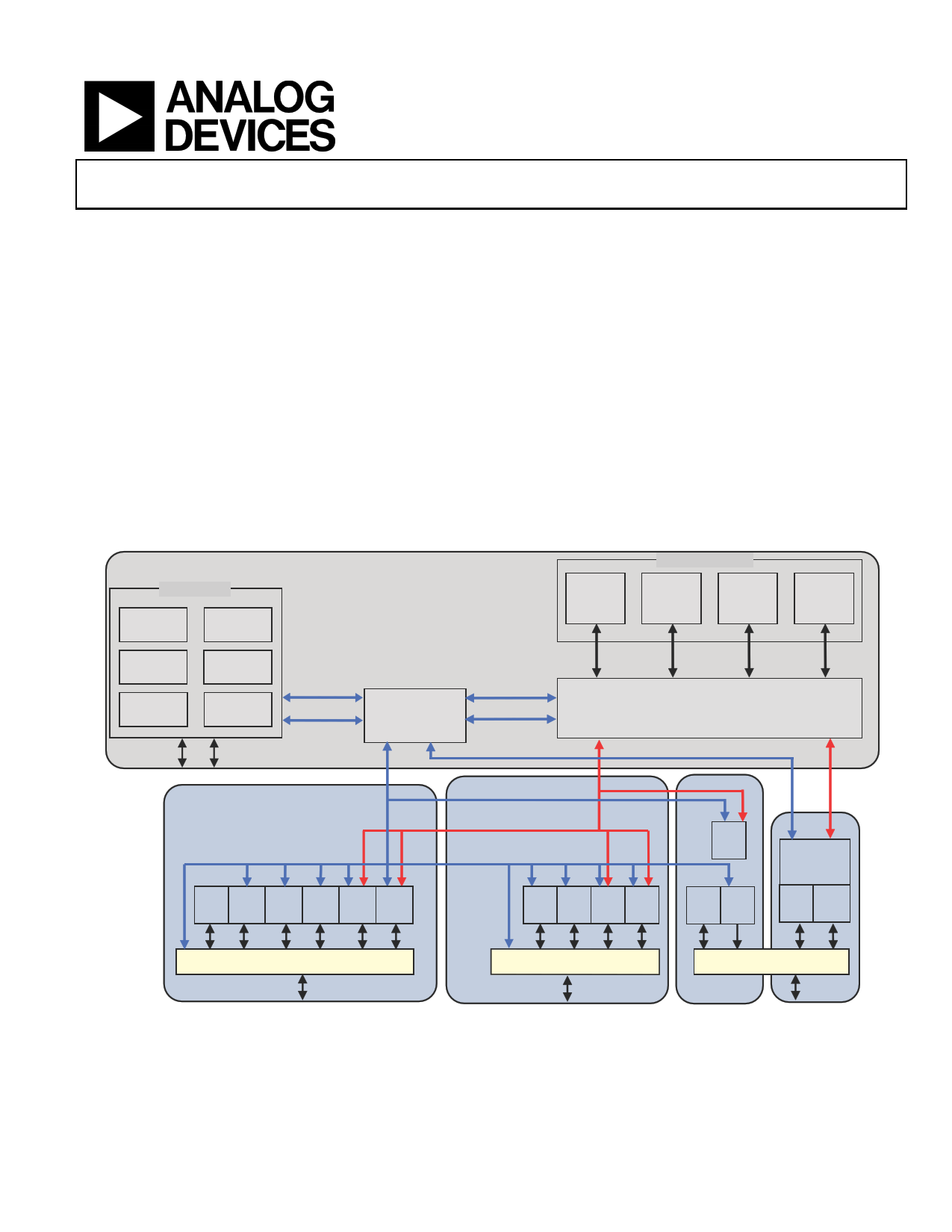
SIMD Core
Instruction
Cache
5 stage
Sequencer
DAG1/2
Timer
PEx PEy
FLAGx/IRQx/
TMREXP
JTAG
Block 0
RAM/ROM
Internal Memory
Block 1
RAM/ROM
Block 2
RAM
Block 3
RAM
S
DMD 64-BIT
PMD 64-BIT
Core Bus
Cross Bar
DMD 64-BIT
PMD 64-BIT
PERIPHERAL BUS
32-BIT
EPD BUS 48-BIT
B0D
64-BIT
B1D
64-BIT
B2D
64-BIT
B3D
64-BIT
Internal Memory I/F
IODO 32-BIT
IOD1
32-BIT
PERIPHERAL BUS
IOD0 BUS
MTM/
D TCP
EP
CORE PCG TIMER
FLAGS C-D
1-0 TWI SPI/B UART
PCG S/PDIF IDP/ SPORT
A-D Tx/Rx PDAP 7-0
7-0
CORE PWM
FLAGS 3-0
AMI SDRAM
DPI Routing/Pins
DPI Peripherals
DAI Routing/Pins
DAI Peripherals
Figure 1. Functional Block Diagram
External Port Pin MUX
Peripherals
External
Port
SHARC and the SHARC logo are registered trademarks of Analog Devices, Inc.
Rev. D
Document Feedback
Information furnished by Analog Devices is believed to be accurate and reliable.
However, no responsibility is assumed by Analog Devices for its use, nor for any
infringements of patents or other rights of third parties that may result from its use.
Specifications subject to change without notice. No license is granted by implication
or otherwise under any patent or patent rights of Analog Devices. Trademarks and
registered trademarks are the property of their respective companies.
One Technology Way, P.O. Box 9106, Norwood, MA 02062-9106 U.S.A.
Tel: 781.329.4700
©2013 Analog Devices, Inc. All rights reserved.
Technical Support
www.analog.com
1 page 
Data Register File
Each processing element contains a general-purpose data regis-
ter file. The register files transfer data between the computation
units and the data buses, and store intermediate results. These
10-port, 32-register (16 primary, 16 secondary) register files,
combined with the SHARC’s enhanced Harvard architecture,
allow unconstrained data flow between computation units and
internal memory. The registers in PEX are referred to as
R0–R15 and in PEY as S0–S15.
Context Switch
Many of the processor’s registers have secondary registers that
can be activated during interrupt servicing for a fast context
switch. The data registers in the register file, the DAG registers,
and the multiplier result register all have secondary registers.
The primary registers are active at reset, while the secondary
registers are activated by control bits in a mode control register.
Universal Registers
Universal registers can be used for general purpose tasks. The
USTAT (4) registers allow easy bit manipulations (Set, Clear,
Toggle, Test, XOR) for all system registers (control/status) of
the core.
The data bus exchange register PX permits data to be passed
between the 64-bit PM data bus and the 64-bit DM data bus, or
between the 40-bit register file and the PM data bus. These reg-
isters contain hardware to handle the data width difference.
Timer
The processors contain a core timer that can generate periodic
software interrupts. The core timer can be configured to use
FLAG3 as a timer expired signal.
Single-Cycle Fetch of an Instruction and Four Operands
The processors feature an enhanced Harvard architecture in
which the data memory (DM) bus transfers data and the pro-
gram memory (PM) bus transfers both instructions and data
(see Figure 2). With the processor’s separate program and data
memory buses and on-chip instruction cache, the processor can
simultaneously fetch four operands (two over each data bus)
and one instruction (from the cache), all in a single cycle.
Instruction Cache
The processors include an on-chip instruction cache that
enables three-bus operation for fetching an instruction and four
data values. The cache is selective—only the instructions whose
fetches conflict with PM bus data accesses are cached. This
cache allows full speed execution of core, looped operations
such as digital filter multiply-accumulates, and FFT butterfly
processing.
Data Address Generators with Zero-Overhead Hardware
Circular Buffer Support
The processors’s two data address generators (DAGs) are used
for indirect addressing and implementing circular data buffers
in hardware. Circular buffers allow efficient programming of
delay lines and other data structures required in digital signal
ADSP-21371/ADSP-21375
processing, and are commonly used in digital filters and Fourier
transforms. The two DAGs contain sufficient registers to allow
the creation of up to 32 circular buffers (16 primary register sets,
16 secondary). The DAGs automatically handle address pointer
wraparound, reduce overhead, increase performance, and sim-
plify implementation. Circular buffers can start and end at any
memory location.
Flexible Instruction Set
The 48-bit instruction word accommodates a variety of parallel
operations, for concise programming. For example, the proces-
sors can conditionally execute a multiply, an add, and a subtract
in both processing elements while branching and fetching up to
four 32-bit values from memory—all in a single instruction.
On-Chip Memory
The ADSP-21371 processor contains 1 megabit of internal RAM
and four megabits of internal mask-programmable ROM (see
Table 3 on Page 6) and the ADSP-21375 processor contains 0.5
megabits of internal RAM and two megabits of internal mask-
programmable ROM (see Table 4 on Page 7). Each block can be
configured for different combinations of code and data storage.
Each memory block supports single-cycle, independent accesses
by the core processor and I/O processor. The processor’s mem-
ory architecture, in combination with its separate on-chip buses,
allow two data transfers from the core and one from the I/O
processor, in a single cycle.
The ADSP-21371 processor’s SRAM can be configured as a
maximum of 32k words of 32-bit data, 64k words of 16-bit data,
21.3k words of 48-bit instructions (or 40-bit data), or combina-
tions of different word sizes up to 1 megabit. All of the memory
can be accessed as 16-bit, 32-bit, 48-bit, or 64-bit words. A 16-
bit floating-point storage format is supported that effectively
doubles the amount of data that may be stored on-chip. Conver-
sion between the 32-bit floating-point and 16-bit floating-point
formats is performed in a single instruction. While each mem-
ory block can store combinations of code and data, accesses are
most efficient when one block stores data using the DM bus for
transfers, and the other block stores instructions and data using
the PM bus for transfers.
Using the DM bus and PM buses, with one bus dedicated to a
memory block, assures single-cycle execution with two data
transfers. In this case, the instruction must be available in
the cache.
On-Chip Memory Bandwidth
The internal memory architecture allows four accesses at the
same time to any of the four blocks, assuming no block con-
flicts. The total bandwidth is gained with DMD and PMD buses
(2 64-bits, core CLK) and the IOD0/1 buses (2 32-bit,
PCLK).
ROM-Based Security
The processors have a ROM security feature that provides hard-
ware support for securing user software code by preventing
unauthorized reading from the internal code when enabled.
When using this feature, the processor does not boot-load any
Rev. D | Page 5 of 56 | April 2013
5 Page 
Power Supplies
The processors have separate power supply connections for the
internal (VDDINT), and external (VDDEXT) power supplies. The
internal supplies must meet the 1.2 V requirement. The external
supply must meet the 3.3 V requirement. All external supply
pins must be connected to the same power supply.
Target Board JTAG Emulator Connector
Analog Devices DSP Tools product line of JTAG emulators uses
the IEEE 1149.1 JTAG test access port of the processor to moni-
tor and control the target board processor during emulation.
Analog Devices DSP Tools product line of JTAG emulators pro-
vides emulation at full processor speed, allowing inspection and
modification of memory, registers, and processor stacks. The
processor’s JTAG interface ensures that the emulator will not
affect target system loading
or timing.
For complete information on Analog Devices’ SHARC DSP
Tools product line of JTAG emulator operation, see the appro-
priate “Emulator Hardware User’s Guide”.
DEVELOPMENT TOOLS
Analog Devices supports its processors with a complete line of
software and hardware development tools, including integrated
development environments (which include CrossCore® Embed-
ded Studio and/or VisualDSP++®), evaluation products,
emulators, and a wide variety of software add-ins.
Integrated Development Environments (IDEs)
For C/C++ software writing and editing, code generation, and
debug support, Analog Devices offers two IDEs.
The newest IDE, CrossCore Embedded Studio, is based on the
EclipseTM framework. Supporting most Analog Devices proces-
sor families, it is the IDE of choice for future processors,
including multicore devices. CrossCore Embedded Studio
seamlessly integrates available software add-ins to support real
time operating systems, file systems, TCP/IP stacks, USB stacks,
algorithmic software modules, and evaluation hardware board
support packages. For more information visit
www.analog.com/cces.
The other Analog Devices IDE, VisualDSP++, supports proces-
sor families introduced prior to the release of CrossCore
Embedded Studio. This IDE includes the Analog Devices VDK
real time operating system and an open source TCP/IP stack.
For more information visit www.analog.com/visualdsp. Note
that VisualDSP++ will not support future Analog Devices
processors.
EZ-KIT Lite Evaluation Board
For processor evaluation, Analog Devices provides wide range
of EZ-KIT Lite® evaluation boards. Including the processor and
key peripherals, the evaluation board also supports on-chip
emulation capabilities and other evaluation and development
features. Also available are various EZ-Extenders®, which are
daughter cards delivering additional specialized functionality,
including audio and video processing. For more information
visit www.analog.com and search on “ezkit” or “ezextender”.
ADSP-21371/ADSP-21375
EZ-KIT Lite Evaluation Kits
For a cost-effective way to learn more about developing with
Analog Devices processors, Analog Devices offer a range of EZ-
KIT Lite evaluation kits. Each evaluation kit includes an EZ-KIT
Lite evaluation board, directions for downloading an evaluation
version of the available IDE(s), a USB cable, and a power supply.
The USB controller on the EZ-KIT Lite board connects to the
USB port of the user’s PC, enabling the chosen IDE evaluation
suite to emulate the on-board processor in-circuit. This permits
the customer to download, execute, and debug programs for the
EZ-KIT Lite system. It also supports in-circuit programming of
the on-board Flash device to store user-specific boot code,
enabling standalone operation. With the full version of Cross-
Core Embedded Studio or VisualDSP++ installed (sold
separately), engineers can develop software for supported EZ-
KITs or any custom system utilizing supported Analog Devices
processors.
Software Add-Ins for CrossCore Embedded Studio
Analog Devices offers software add-ins which seamlessly inte-
grate with CrossCore Embedded Studio to extend its capabilities
and reduce development time. Add-ins include board support
packages for evaluation hardware, various middleware pack-
ages, and algorithmic modules. Documentation, help,
configuration dialogs, and coding examples present in these
add-ins are viewable through the CrossCore Embedded Studio
IDE once the add-in is installed.
Board Support Packages for Evaluation Hardware
Software support for the EZ-KIT Lite evaluation boards and EZ-
Extender daughter cards is provided by software add-ins called
Board Support Packages (BSPs). The BSPs contain the required
drivers, pertinent release notes, and select example code for the
given evaluation hardware. A download link for a specific BSP is
located on the web page for the associated EZ-KIT or EZ-
Extender product. The link is found in the Product Download
area of the product web page.
Middleware Packages
Analog Devices separately offers middleware add-ins such as
real time operating systems, file systems, USB stacks, and
TCP/IP stacks. For more information see the following web
pages:
• www.analog.com/ucos3
• www.analog.com/ucfs
• www.analog.com/ucusbd
• www.analog.com/lwip
Algorithmic Modules
To speed development, Analog Devices offers add-ins that per-
form popular audio and video processing algorithms. These are
available for use with both CrossCore Embedded Studio and
VisualDSP++. For more information visit www.analog.com
and search on “Blackfin software modules” or “SHARC software
modules”.
Rev. D | Page 11 of 56 | April 2013
11 Page | ||
| Páginas | Total 30 Páginas | |
| PDF Descargar | [ Datasheet ADSP-21375.PDF ] | |
Hoja de datos destacado
| Número de pieza | Descripción | Fabricantes |
| ADSP-21371 | SHARC Processor | Analog Devices |
| ADSP-21375 | SHARC Processor | Analog Devices |
| Número de pieza | Descripción | Fabricantes |
| SLA6805M | High Voltage 3 phase Motor Driver IC. |
Sanken |
| SDC1742 | 12- and 14-Bit Hybrid Synchro / Resolver-to-Digital Converters. |
Analog Devices |
|
DataSheet.es es una pagina web que funciona como un repositorio de manuales o hoja de datos de muchos de los productos más populares, |
| DataSheet.es | 2020 | Privacy Policy | Contacto | Buscar |