|
|
PDF ADA4862-3 Data sheet ( Hoja de datos )
| Número de pieza | ADA4862-3 | |
| Descripción | Triple Op Amp | |
| Fabricantes | Analog Devices | |
| Logotipo |  |
|
Hay una vista previa y un enlace de descarga de ADA4862-3 (archivo pdf) en la parte inferior de esta página. Total 16 Páginas | ||
|
No Preview Available !
www.DataSheet4U.com
FEATURES
Ideal for RGB/HD/SD video
Supports 1080i/720p resolution
High speed
−3 dB bandwidth: 300 MHz
Slew rate: 750 V/μs
Settling time: 9 ns ( 0.5%)
0.1 dB flatness: 65 MHz
Differential gain: 0.02%
Differential phase: 0.03°
Wide supply range: 5 V to 12 V
Low power: 5.3 mA/amp
Low voltage offset (RTO): 3.5 mV (typ)
High output current: 25 mA
Also configurable for gains of +1, −1
Power-down
APPLICATIONS
Consumer video
Professional video
Filter buffers
GENERAL DESCRIPTION
The ADA4862-3 (triple) is a low cost, high speed, internally
fixed, G = +2 op amp, which provides excellent overall
performance for high definition and RGB video applications.
The 300 MHz, G = +2, −3 dB bandwidth, and 750 V/μs slew
rate make this amplifier well suited for many high speed
applications. The ADA4862-3 can also be configured to
operate in gains of G = +1 and G = −1.
With its combination of low price, excellent differential gain
(0.02%), differential phase (0.03°), and 0.1 dB flatness out to
65 MHz, this amplifier is ideal for both consumer and
professional video applications.
The ADA4862-3 is designed to operate on supply voltages as
low as +5 V and up to ±5 V using only 5.3 mA/amp of supply
current. To further reduce power consumption, each amplifier
is equipped with a power-down feature that lowers the supply
current to 200 μA/amp. The ADA4862-3 also consumes less
board area because feedback and gain set resistors are on-chip.
Having the resistors on chip simplifies layout and minimizes the
required board space.
High Speed, G = +2,
Low Cost, Triple Op Amp
ADA4862-3
PIN CONFIGURATION
POWER DOWN 1 1
550Ω
14 VOUT2
POWER DOWN 2 2
POWER DOWN 3 3
550Ω 13 –IN 2
12 +IN 2
+VS 4
ADA4862-3
11 –VS
+IN 1 5
–IN 1 6
550Ω
550Ω
10 +IN 3
9 –IN 3
VOUT1 7
550Ω
550Ω
8 VOUT3
Figure 1. 14-Lead SOIC (R-14)
The ADA4862-3 is available in a 14-lead SOIC package and is
designed to work in the extended temperature range of −40°C
to +105°C.
6.1
6.0
5.9
5.8
G = +2
RL = 150Ω
5.7
CL = 4pF
VOUT = 2V p-p
5.6
VS = ±5V
VS = +5V
5.5
5.4
5.3
5.2
5.1
0.1
1 10 100
FREQUENCY (MHz)
1000
Figure 2. Large Signal 0.1 dB Bandwidth for Various Supplies
Rev. A
Information furnished by Analog Devices is believed to be accurate and reliable. However, no
responsibility is assumed by Analog Devices for its use, nor for any infringements of patents or other
rights of third parties that may result from its use. Specifications subject to change without notice. No
license is granted by implication or otherwise under any patent or patent rights of Analog Devices.
Trademarksandregisteredtrademarksarethepropertyoftheirrespectiveowners.
One Technology Way, P.O. Box 9106, Norwood, MA 02062-9106, U.S.A.
Tel: 781.329.4700
www.analog.com
Fax: 781.461.3113
© 2005 Analog Devices, Inc. All rights reserved.
1 page 
ABSOLUTE MAXIMUM RATINGS
Table 3.
Parameter
Supply Voltage
Power Dissipation
Common-Mode Input Voltage
Storage Temperature
Operating Temperature Range
Lead Temperature
Junction Temperature
Rating
12.6 V
See Figure 3
±VS
−65°C to +125°C
−40°C to +105°C
JEDEC J-STD-20
150°C
Stresses above those listed under Absolute Maximum Ratings
may cause permanent damage to the device. This is a stress
rating only; functional operation of the device at these or any
other conditions above those indicated in the operational
section of this specification is not implied. Exposure to absolute
maximum rating conditions for extended periods may affect
device reliability.
THERMAL RESISTANCE
θJA is specified for the worst-case conditions, that is, θJA is
specified for device soldered in circuit board for surface-mount
packages.
Table 4. Thermal Resistance
Package Type
14-lead SOIC
θJA
90
Unit
°C/W
Maximum Power Dissipation
The maximum safe power dissipation for the ADA4862-3 is
limited by the associated rise in junction temperature (TJ) on
the die. At approximately 150°C, which is the glass transition
temperature, the plastic changes its properties. Even
temporarily exceeding this temperature limit may change the
stresses that the package exerts on the die, permanently shifting
the parametric performance of the amplifiers. Exceeding a
junction temperature of 150°C for an extended period can
result in changes in silicon devices, potentially causing
degradation or loss of functionality.
ADA4862-3
The power dissipated in the package (PD) is the sum of the
quiescent power dissipation and the power dissipated in the die due
to the amplifier’s drive at the output. The quiescent power is the
voltage between the supply pins (VS) × the quiescent current (IS).
PD = Quiescent Power + (Total Drive Power − Load Power)
PD
= (VS
×
I
S
)
+
⎜⎛
⎝
VS
2
× VOUT
RL
⎟⎞
⎠
–
VOUT
RL
2
RMS output voltages should be considered.
Airflow increases heat dissipation, effectively reducing θJA.
In addition, more metal directly in contact with the package
leads and through holes under the device reduces θJA.
Figure 3 shows the maximum safe power dissipation in the
package vs. the ambient temperature for the 14-lead SOIC
(90°C/W) on a JEDEC standard 4-layer board. θJA values are
approximations.
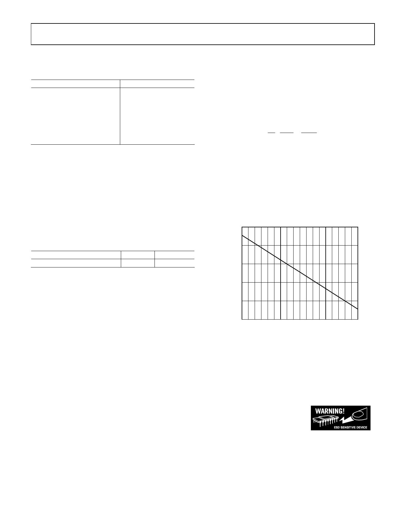
2.5
2.0
1.5
1.0
0.5
0
–55 –45 –35 –25 –15 –5 5 15 25 35 45 55 65 75 85 95 105 115 125
AMBIENT TEMPERATURE (°C)
Figure 3. Maximum Power Dissipation vs. Temperature for a 4-Layer Board
ESD CAUTION
ESD (electrostatic discharge) sensitive device. Electrostatic charges as high as 4000 V readily accumulate on
the human body and test equipment and can discharge without detection. Although this product features
proprietary ESD protection circuitry, permanent damage may occur on devices subjected to high energy
electrostatic discharges. Therefore, proper ESD precautions are recommended to avoid performance
degradation or loss of functionality.
Rev. A | Page 5 of 16
5 Page 
APPLICATIONS
USING THE ADA4862-3 IN GAINS = +1, −1
The ADA4862-3 was designed to offer outstanding video
performance, simplify applications, and minimize board area.
The ADA4862-3 is a triple amplifier with on-chip feedback and
gain set resistors. The gain is fixed internally at G = +2. The
inclusion of the on-chip resistors not only simplifies the design
of the application but also eliminates six surface-mount
resistors, saving valuable board space and lowers assembly
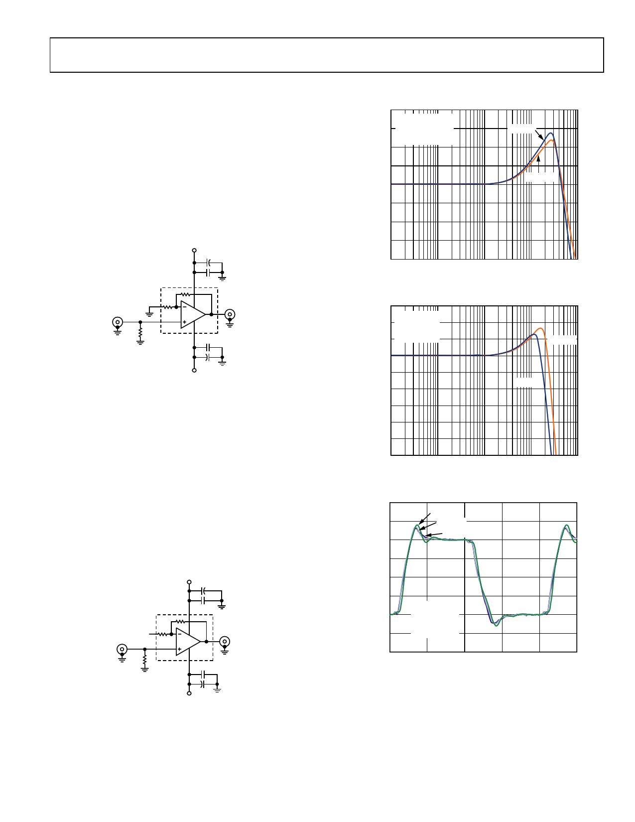
costs. A typical schematic is shown in Figure 29.
+VS
10μF
0.01μF
VIN
RT
0.01μF
VOUT
10μF
–VS
GAIN OF +2
Figure 29. Noninverting Configuration (G = +2)
While the ADA4862-3 has a fixed gain of G = +2, it can be used
in other gain configurations, such as G = −1 and G = +1, which
are discussed next.
Unity-Gain Operation (Option 1)
There are two options for obtaining unity gain (G = +1). The
first is shown in Figure 30. In this configuration, the –IN input
pin is left floating (feedback is provided via the internal 550 Ω),
and the input is applied to the noninverting input. The noise
gain for this configuration is 1. Frequency performance and
transient response are shown in Figure 31 through Figure 33.
+VS
10μF
0.01μF
VIN
RT
VOUT
0.01μF
10μF
–VS
GAIN OF +1
Figure 30. Unity Gain of Option 1
ADA4862-3
4
G = +1
3
RL = 150Ω
CL = 4pF
VOUT = 200mV p-p
2
VS = +5V
1
VS = ±5V
0
–1
–2
–3
–4
0.1
1 10 100
FREQUENCY (MHz)
Figure 31. Small Signal Unity Gain
1000
3
G = +1
2 RL = 150Ω
CL = 4pF
1 VOUT = 2V p-p
0
VS = ±5V
–1
VS = +5V
–2
–3
–4
–5
–6
0.1
1 10 100
FREQUENCY (MHz)
Figure 32. Large Signal Gain +1
1000
2.0
CL = 9pF
1.5 CL = 6pF
CL = 4pF
1.0
0.5
0
–0.5
G = +1
–1.0
–1.5
RL = 150Ω
VOUT = 2V p-p
VS = ±5V
TIME = 5ns/DIV
–2.0
Figure 33. Large Signal Transient Response for Various Capacitor Loads
Rev. A | Page 11 of 16
11 Page | ||
| Páginas | Total 16 Páginas | |
| PDF Descargar | [ Datasheet ADA4862-3.PDF ] | |
Hoja de datos destacado
| Número de pieza | Descripción | Fabricantes |
| ADA4862-3 | Triple Op Amp | Analog Devices |
| Número de pieza | Descripción | Fabricantes |
| SLA6805M | High Voltage 3 phase Motor Driver IC. |
Sanken |
| SDC1742 | 12- and 14-Bit Hybrid Synchro / Resolver-to-Digital Converters. |
Analog Devices |
|
DataSheet.es es una pagina web que funciona como un repositorio de manuales o hoja de datos de muchos de los productos más populares, |
| DataSheet.es | 2020 | Privacy Policy | Contacto | Buscar |
