|
|
|
PDF VSC7216-01 Data sheet ( Hoja de datos )
| Número de pieza | VSC7216-01 | |
| Descripción | Multi-Gigabit Interconnect Chip | |
| Fabricantes | Vitesse Semiconductor | |
| Logotipo | ||
Hay una vista previa y un enlace de descarga de VSC7216-01 (archivo pdf) en la parte inferior de esta página. Total 30 Páginas | ||
|
No Preview Available !
www.DataSheet4U.com
VITESSE
SEMICONDUCTOR CORPORATION
Preliminary Datasheet
VSC7216-01
Multi-Gigabit Interconnect Chip
Features
• 4 ANSI X3T11 Fibre Channel and IEEE 802.3z
Gigabit Ethernet Compliant Transceivers
• Received Data Aligned to Local REFCLK or to
Recovered Clock
• Over 8 Gb/s Duplex Raw Data Rate
• PECL Rx Signal Detect and Cable Equalization
• Redundant PECL Tx Outputs and Rx Inputs
• 8B/10B Encoder/Decoder per Channel, Optional
Encoder/Decoder Bypass Operation
• Per-Channel Serial Tx-to-Rx and Parallel Rx-
to-Tx Internal Loopback Modes
• Clock Multiplier Generates Baud Rate Clock
• “ASIC-FriendlyTM” Timing Options for Transmitter
Parallel Input Data
• Elastic Buffers for Intra/Inter-Chip Cable Deskewing
and Channel-to-Channel Alignment
• Tx/Rx Rate Matching via IDLE Insertion/Deletion
• Compatible with VSC7211/7212/7214
• Automatic Lock-to-Reference
• JTAG Boundary Scan Support for TTL I/O
• Built-In Self Test
• 3.3V Supply, 3.0W
• 256-Pin, 27mm BGA package
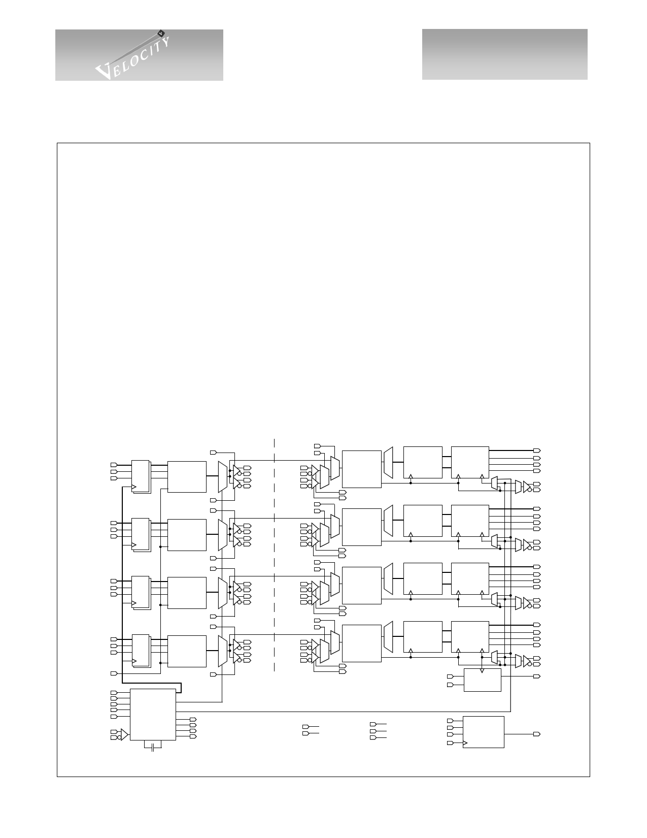
VSC7216-01 Block Diagram
TD(7:0)
C/DD
WSEND
TC(7:0)
C/DC
WSENC
TB(7:0)
C/DB
WSENB
TA(7:0)
C/DA
WSENA
KCHAR
TBCA
TBCB
TBCC
TBCD
DUAL
REFCLKP
REFCLKN
TRANSMITTER
88
DQ
PTXEND
8B/10B 10
Encode
LBTXD
LBEND(1:0)
RXP/RD
PTXD+ PRXD+
PTXD- PRXD-
RTXD+ RRXD+
RTXD- RRXD-
88
DQ
RTXEND
PTXENC
8B/10B 10
Encode
LBTXC
LBENC(1:0)
RXP/RC
PTXC+ PRXC+
PTXC- PRXC-
RTXC+ RRXC+
RTXC- RRXC-
88
DQ
RTXENC
PTXENB
8B/10B 10
Encode
LBTXB
LBENB(1:0)
RXP/RB
PTXB+ PRXB+
PTXB- PRXB-
RTXB+ RRXB+
RTXB- RRXB-
88
DQ
RTXENB
PTXENA
8B/10B 10
Encode
LBTXA
LBENA(1:0)
RXP/RA
PTXA+ PRXA+
PTXA- PRXA-
RTXA+ RRXA+
RTXA- RRXA-
RTXENA
4
x20/x10
Clock Gen
CAP0 CAP1
Tx Clock
REFCLK
TBERRA
TBERRB
TBERRC
TBERRD
TMODE(2:0)
RMODE(1:0)
RECEIVER
Clk/Data
Recovery
8
10 8B/10B 8 Elastic
Decode 3 Buffer
PSDETD
RSDETD
Clk/Data
Recovery
8
10 8B/10B 8 Elastic
Decode 3 Buffer
PSDETC
RSDETC
Clk/Data
Recovery
8
10 8B/10B 8 Elastic
Decode 3 Buffer
PSDETB
RSDETB
Clk/Data
Recovery
8
10 8B/10B 8 Elastic
Decode 3 Buffer
PSDETA
RSDETA
WSI
FLOCK
Channel
Align
RESETN
ENDEC
BIST
TRSTN
TMS
TDI
TCK
JTAG
Boundary
Scan
RD(7:0)
IDLED
KCHD
ERRD
RCLKD
RCLKDN
RC7:0)
IDLEC
KCHC
ERRC
RCLKC
RCLKCN
RB(7:0)
IDLEB
KCHB
ERRB
RCLKB
RCLKBN
RA(7:0)
IDLEA
KCHA
ERRD
RCLKA
RCLKAN
WSO
TDO
G52352-0, Rev 3.2
05/05/01
© VITESSE SEMICONDUCTOR CORPORATION • 741 Calle Plano • Camarillo, CA 93012
Tel: (800) VITESSE • FAX: (805) 987-5896 • Email: [email protected]
Internet: www.vitesse.com
Page 1
1 page 
VITESSE
SEMICONDUCTOR CORPORATION
Preliminary Datasheet
VSC7216-01
Multi-Gigabit Interconnect Chip
Figure 4: Transmit Timing, TMODE(2:0) = 11X (“ASIC-Friendly” Timing)
0o
90o
180o
270o
360o
TBCA
or
TBCn
Tn(7:0)
C/Dn
WSENn
Valid
Valid
Valid
8B/10B Encoder
Each channel contains an 8B/10B encoder which translates the 8-bit input data on Tn(7:0) into a 10-bit
encoded data character. C/Dn inputs are also provided in each channel which, along with KCHAR, allow the
transmission of special Fibre Channel Kxx.x characters (see Table 3). Note that KCHAR is a static input, and
does NOT have the same input timing as Tn(7:0), C/Dn and WSENn. Normally C/Dn is LOW in order to
transmit data. If C/Dn is HIGH and KCHAR is LOW, then a Fibre Channel defined IDLE Character (K28.5 =
‘0011111010’ or ‘1100000101’ depending on disparity) is transmitted and Tn(7:0) is ignored. If C/Dn is HIGH
and KCHAR is HIGH, a Kxx.x character is transmitted as determined by the data pattern on Tn(7:0) (see Table
4). Data patterns other than those defined in Table 4 produce undefined 10B encodings.
Table 3: Transmit Data Controls
WSENn
0
0
0
1
C/Dn
0
1
1
X
KCHAR
X
0
1
X
Encoded 10-Bit Output
Data Character
IDLE Character (K28.5)
Special Kxx.x Character
16-Character Word Sync Sequence
Table 4: Special Characters (Selected when C/Dn and KCHAR are HIGH)
Code
K28.0
K28.1
K28.2
K28.3
K28.4
K28.5
K28.5+
Tn(7:0)
000 11100
001 11100
010 11100
011 11100
100 11100
101 11100
101 01100
Comment
User Defined
User Defined
User Defined
User Defined
User Defined
IDLE
User Defined
Code
K28.5-
K28.6
K28.7
K23.7
K27.7
K29.7
K30.7
Tn(7:0)
101 01101
110 11100
111 11100
111 10111
111 11011
111 11101
111 11110
Comment
User Defined
User Defined
Test Only
User Defined
User Defined
User Defined
User Defined
G52352-0, Rev 3.2
05/05/01
© VITESSE SEMICONDUCTOR CORPORATION • 741 Calle Plano • Camarillo, CA 93012
Internet: www.vitesse.com
Page 5
5 Page 
VITESSE
SEMICONDUCTOR CORPORATION
Preliminary Datasheet
VSC7216-01
Multi-Gigabit Interconnect Chip
The data coming from the decoder is clocked into the elastic buffer by the recovered clock from the
channel’s CRU. The data is clocked out of the elastic buffers with word clock. If the transmitting device’s
REFCLK is not precisely frequency-locked to a receive channel’s word clock, the channel’s elastic buffer will
tend to gradually fill or empty as the recovered clock (which is by definition frequency-locked to the
transmitter’s REFCLK) steadily drifts in phase relative to the word clock.
In order to accommodate frequency differences between a transmitter’s REFCLK and the word clock, the
VSC7216-01 can automatically perform rate matching by either deleting or duplicating IDLE characters. The
FLOCK input must be LOW to enable rate matching which, based on how the WSI input is connected, can
either be performed in each channel individually or can be performed in parallel across a group of channels that
are word-aligned. This is discussed in detail in the Word Alignment section below. It is the user’s responsibility
to ensure that the frequency at which IDLEs are simultaneously transmitted on each channel accommodates the
frequency differences, if any, in their system architecture. Not meeting the IDLE density requirements could
result in Underrun/Overrun Errors. However, the use of a continuous stream of IDLE characters should be
avoided when rate matching is enable. The IDLE addition/deletion logic relies on the status bits (see Table 8 for
details) to identify K28.5 IDLE characters. The use of continuous IDLE characters will force the VSC7216-01
into the RESYNC state (see Figure 9) resulting in a status bit sequence which the addition/deletion logic does
not recognize as an IDLE character.
The elastic buffer is designed to allow a maximum phase drift of +2 or -2 serial clock bit times between re-
synchronizations, which sets a limit on the maximum data “packet” length allowed between IDLEs. This
maximum packet length depends on the frequency difference between the transmitting and receiving device’s
REFCLKs. Let ∆φ represent phase drift in bit times, and let 2π represent one full 10-bit character of phase
drift. Limiting phase drift to two bit times means the following inequality must be satisfied:
(1) ∆φ ≤ (0.2 × 2π)
Let L be the number of 10-bit characters transmitted, and let ∆f be the frequency offset in ppm. The total
phase drift in bit times is given by:
(2) ∆φ = (∆f ⁄ 106) × 2πL
A simple expression for maximum packet length as a function of frequency offset is derived by substituting
(2) in (1) and solving for L:
(3) L ≤ (0.2 × 10⁶) ⁄ ∆f
As an example, if the frequency offset is 200ppm, the maximum packet length should not be more than 1K
bytes. To increase the maximum packet length L, decrease the frequency offset ∆f. Please note that if only one
K28.5 is transmitted between “packets” of data, it might be dropped during compensation for phase drift. If the
user must have at least one K28.5 between these two packets, then two K28.5s must be transmitted.
Word Alignment
The VSC7216-01 performs channel-to-channel word alignment. In this mode of operation, if the data from
all four channels on the transmitting VSC7216-01 (e.g., the 4 Tn(7:0) busses) is viewed as a 32-bit word, then
the receiving VSC7216-01 will recover an identical word. For example, if a transmit pattern was ‘ABCD’,
G52352-0, Rev 3.2
05/05/01
© VITESSE SEMICONDUCTOR CORPORATION • 741 Calle Plano • Camarillo, CA 93012
Internet: www.vitesse.com
Page 11
11 Page | ||
| Páginas | Total 30 Páginas | |
| PDF Descargar | [ Datasheet VSC7216-01.PDF ] | |
Hoja de datos destacado
| Número de pieza | Descripción | Fabricantes |
| VSC7216-01 | Multi-Gigabit Interconnect Chip | Vitesse Semiconductor |
| Número de pieza | Descripción | Fabricantes |
| SLA6805M | High Voltage 3 phase Motor Driver IC. |
Sanken |
| SDC1742 | 12- and 14-Bit Hybrid Synchro / Resolver-to-Digital Converters. |
Analog Devices |
|
DataSheet.es es una pagina web que funciona como un repositorio de manuales o hoja de datos de muchos de los productos más populares, |
| DataSheet.es | 2020 | Privacy Policy | Contacto | Buscar |