|
|
|
PDF DS26524 Data sheet ( Hoja de datos )
| Número de pieza | DS26524 | |
| Descripción | Quad T1/E1/J1 Transceiver | |
| Fabricantes | Maxim Integrated Products | |
| Logotipo | ||
Hay una vista previa y un enlace de descarga de DS26524 (archivo pdf) en la parte inferior de esta página. Total 30 Páginas | ||
|
No Preview Available !
www.DataSheet4U.com
www.maxim-ic.com
GENERAL DESCRIPTION
The DS26524 is a single-chip 4-port framer and line
interface unit (LIU) combination for T1, E1, and J1
applications. Each channel is independently
configurable, supporting both long-haul and short-haul
lines.
APPLICATIONS
Routers
Channel Service Units (CSUs)
Data Service Units (DSUs)
Muxes
Switches
Channel Banks
T1/E1 Test Equipment
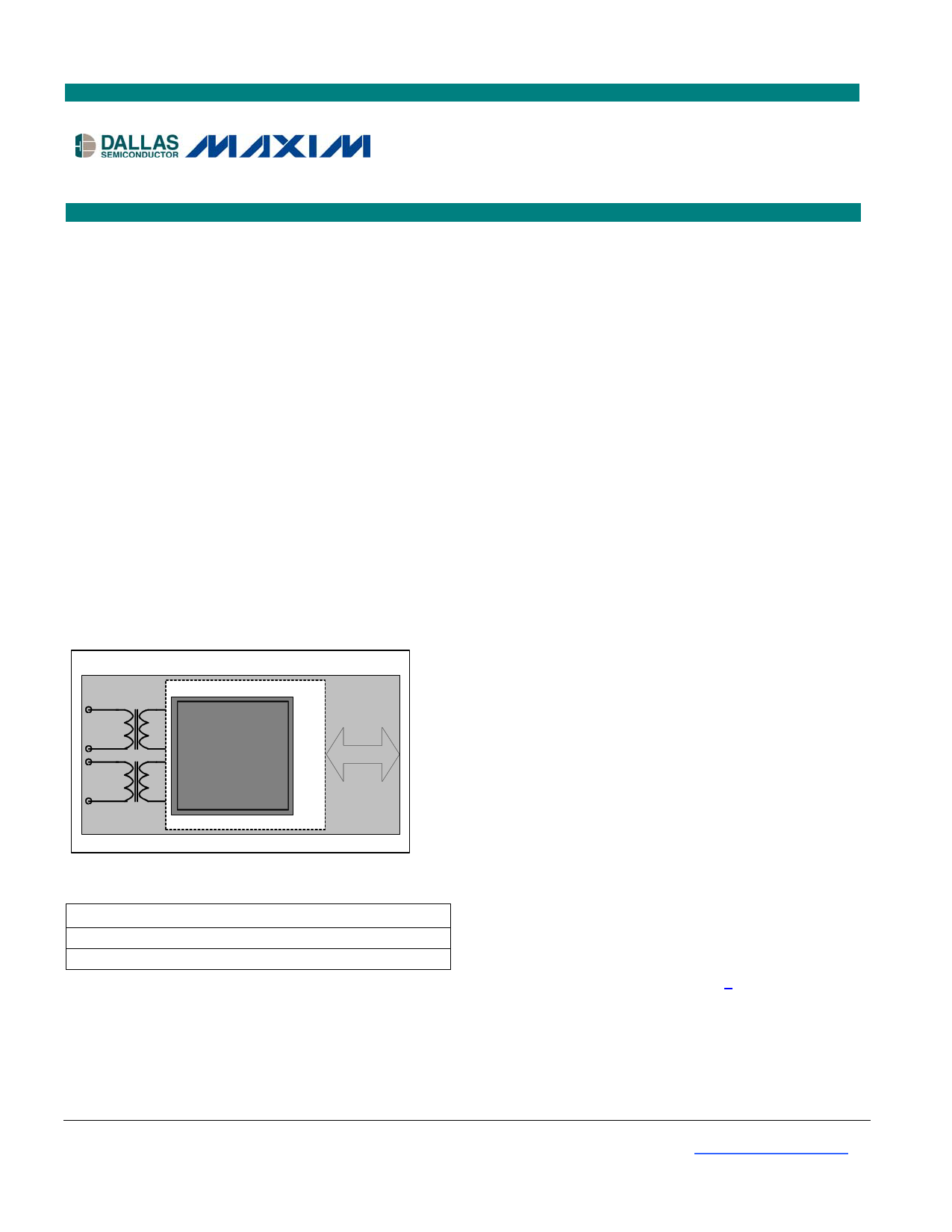
TYPICAL OPERATING CIRCUIT
T1/E1/J1
NETWORK
DS26524
T1/J1/E1
Transceiver x4 BACKPLANE
TDM
ORDERING INFORMATION
PART
DS26524GN
DS26524GN+
TEMP RANGE
-40°C to +85°C
-40°C to +85°C
PIN-PACKAGE
256 TE-CSBGA
256 TE-CSBGA
+ Denotes lead-free/RoHS compliant device.
DS26524
Quad T1/E1/J1 Transceiver
FEATURES
Four Complete T1, E1, or J1 Long-Haul/Short-
Haul Transceivers (LIU plus Framer)
Independent T1, E1, or J1 Selections for Each
Transceiver
Internal Software-Selectable Transmit- and
Receive-Side Termination for 100Ω T1 Twisted
Pair, 110Ω J1 Twisted Pair, 120Ω E1 Twisted
Pair, and 75Ω E1 Coaxial Applications
Crystal-Less Jitter Attenuator can be Selected
for Transmit or Receive Path; Jitter Attenuator
Meets ETS CTR 12/13, ITU-T G.736, G.742,
G.823, and AT&T Pub 62411
External Master Clock can be Multiple of
2.048MHz or 1.544MHz for T1/J1 or E1
Operation; This Clock is Internally Adapted for
T1 or E1 Usage in the Host Mode
Receive-Signal Level Indication from -2.5dB to
-36dB in T1 Mode and -2.5dB to -44dB in E1
Mode in Approximate 2.5dB Increments
Transmit Open- and Short-Circuit Detection
LIU LOS in Accordance with G.775, ETS 300
233, and T1.231
Transmit Synchronizer
Flexible Signaling Extraction and Insertion
Using Either the System Interface or
Microprocessor Port
Alarm Detection and Insertion
T1 Framing Formats of D4, SLC-96, and ESF
J1 Support
E1 G.704 and CRC-4 Multiframe
T1-to-E1 Conversion
Features Continued in Section 2.
Note: Some revisions of this device may incorporate deviations from published specifications known as errata. Multiple revisions of any device
may be simultaneously available through various sales channels. For information about device errata, click here: www.maxim-ic.com/errata.
1 of 273
REV: 102106
1 page 
DS26524 Quad T1/E1/J1 Transceiver
LIST OF FIGURES
Figure 6-1. Block Diagram ......................................................................................................................................... 17
Figure 6-2. Detailed Block Diagram........................................................................................................................... 18
Figure 8-1. Backplane Clock Generation................................................................................................................... 27
Figure 8-2. Device Interrupt Information Flow Diagram............................................................................................. 30
Figure 8-3. IBO Multiplexer Equivalent Circuit—4.096MHz ...................................................................................... 35
Figure 8-4. IBO Multiplexer Equivalent Circuit—8.192MHz ...................................................................................... 36
Figure 8-5. IBO Multiplexer Equivalent Circuit—16.384MHz .................................................................................... 37
Figure 8-6. RSYNC Input in H.100 (CT Bus) Mode................................................................................................... 40
Figure 8-7. TSSYNCIO (Input Mode) Input in H.100 (CT Bus) Mode ....................................................................... 41
Figure 8-8. CRC-4 Recalculate Method .................................................................................................................... 62
Figure 8-9. Receive HDLC Example.......................................................................................................................... 68
Figure 8-10. HDLC Message Transmit Example....................................................................................................... 70
Figure 8-11. Network Connection for Software-Selected Termination—Longitudinal Protection ............................. 72
Figure 8-12. T1/J1 Transmit Pulse Templates .......................................................................................................... 76
Figure 8-13. E1 Transmit Pulse Templates ............................................................................................................... 77
Figure 8-14. Typical Monitor Application ................................................................................................................... 79
Figure 8-15. Jitter Attenuation ................................................................................................................................... 81
Figure 8-16. Analog Loopback................................................................................................................................... 82
Figure 8-17. Local Loopback ..................................................................................................................................... 82
Figure 8-18. Remote Loopback ................................................................................................................................. 83
Figure 8-19. Dual Loopback ...................................................................................................................................... 83
Figure 9-1. Register Memory Map for the DS26524.................................................................................................. 87
Figure 10-1. T1 Receive-Side D4 Timing ................................................................................................................ 233
Figure 10-2. T1 Receive-Side ESF Timing.............................................................................................................. 233
Figure 10-3. T1 Receive-Side Boundary Timing (Elastic Store Disabled)............................................................... 234
Figure 10-4. T1 Receive-Side 1.544MHz Boundary Timing (Elastic Store Enabled).............................................. 234
Figure 10-5. T1 Receive-Side 2.048MHz Boundary Timing (Elastic Store Enabled).............................................. 235
Figure 10-6. T1 Receive-Side Interleave Bus Operation—BYTE Mode.................................................................. 236
Figure 10-7. T1 Receive-Side Interleave Bus Operation—FRAME Mode .............................................................. 237
Figure 10-8. T1 Transmit-Side D4 Timing ............................................................................................................... 238
Figure 10-9. T1 Transmit-Side ESF Timing............................................................................................................. 238
Figure 10-10. T1 Transmit-Side Boundary Timing (Elastic Store Disabled)............................................................ 239
Figure 10-11. T1 Transmit-Side 1.544MHz Boundary Timing (Elastic Store Enabled)........................................... 239
Figure 10-12. T1 Transmit-Side 2.048MHz Boundary Timing (Elastic Store Enabled)........................................... 240
Figure 10-13. T1 Transmit-Side Interleave Bus Operation—BYTE Mode............................................................... 241
Figure 10-14. T1 Transmit Interleave Bus Operation—FRAME Mode.................................................................... 242
Figure 10-15. E1 Receive-Side Timing.................................................................................................................... 243
Figure 10-16. E1 Receive-Side Boundary Timing (Elastic Store Disabled) ............................................................ 243
Figure 10-17. E1 Receive-Side 1.544MHz Boundary Timing (Elastic Store Enabled)............................................ 244
Figure 10-18. E1 Receive-Side 2.048MHz Boundary Timing (Elastic Store Enabled)............................................ 244
Figure 10-19. E1 Transmit-Side Timing................................................................................................................... 245
Figure 10-20. E1 Transmit-Side Boundary Timing (Elastic Store Disabled) ........................................................... 245
Figure 10-21. E1 Transmit-Side 1.544MHz Boundary Timing (Elastic Store Enabled)........................................... 246
Figure 10-22. E1 Transmit-Side 2.048MHz Boundary Timing (Elastic Store Enabled)........................................... 246
Figure 10-23. E1 G.802 Timing ............................................................................................................................... 247
Figure 12-1. Intel Bus Read Timing (BTS = 0) ........................................................................................................ 251
Figure 12-2. Intel Bus Write Timing (BTS = 0)......................................................................................................... 251
Figure 12-3. Motorola Bus Read Timing (BTS = 1) ................................................................................................. 252
5 of 273
5 Page 
DS26524 Quad T1/E1/J1 Transceiver
Detailed alarm and status reporting with optional interrupt support
Large path and line error counters
− T1: BPV, CV, CRC-6, and framing bit errors
− E1: BPV, CV, CRC-4, E-bit, and frame alignment errors
− Timed or manual update modes
DS1 Idle Code Generation on a per-channel basis in both transmit and receive paths
− User defined
− Digital Milliwatt
ANSI T1.403-1999 support
G.965 V5.2 link detect
Ability to monitor one DS0 channel in both the transmit and receive paths
In-band repeating pattern generators and detectors
− Three independent generators and detectors
− Patterns from 1 to 8 bits or 16 bits in length
Bit-oriented code (BOC) support
Flexible signaling support
− Software or hardware based
− Interrupt generated on change of signaling data
− Optional receive-signaling freeze on loss of frame, loss of signal, or frame slip
− Hardware pins provided to indicate loss of frame (LOF), loss of signal (LOS), loss of transmit clock
(LOTC), or signaling freeze condition
Automatic RAI generation to ETS 300 011 specifications
RAI-CI and AIS-CI support
Expanded access to Sa and Si bits
Option to extend carrier loss criteria to a 1ms period as per ETS 300 233
Japanese J1 support
Ability to calculate and check CRC-6 according to the Japanese standard
Ability to generate Yellow Alarm according to the Japanese standard
T1-to-E1 conversion
2.6 System Interface
Independent two-frame receive and transmit elastic stores
Independent control and clocking
Controlled slip capability with status
Minimum delay mode supported
Flexible TDM backplane supports bus rates from 1.544MHz to 16.384MHz
Supports T1 to CEPT (E1) conversion
Programmable output clocks for fractional T1, E1, H0, and H12 applications
Interleaving PCM bus operation
Hardware signaling capability
Receive-signaling reinsertion to a backplane multiframe sync
Availability of signaling in a separate PCM data stream
Signaling freezing
Ability to pass the T1 F-bit position through the elastic stores in the 2.048MHz backplane mode
User-selectable synthesized clock output
11 of 273
11 Page | ||
| Páginas | Total 30 Páginas | |
| PDF Descargar | [ Datasheet DS26524.PDF ] | |
Hoja de datos destacado
| Número de pieza | Descripción | Fabricantes |
| DS26522 | Dual T1/E1/J1 Transceiver | Maxim Integrated Products |
| DS26524 | Quad T1/E1/J1 Transceiver | Maxim Integrated Products |
| DS26528 | Octal T1/E1/J1 Transceiver | Maxim Integrated Products |
| Número de pieza | Descripción | Fabricantes |
| SLA6805M | High Voltage 3 phase Motor Driver IC. |
Sanken |
| SDC1742 | 12- and 14-Bit Hybrid Synchro / Resolver-to-Digital Converters. |
Analog Devices |
|
DataSheet.es es una pagina web que funciona como un repositorio de manuales o hoja de datos de muchos de los productos más populares, |
| DataSheet.es | 2020 | Privacy Policy | Contacto | Buscar |