|
|
|
PDF INA202 Data sheet ( Hoja de datos )
| Número de pieza | INA202 | |
| Descripción | (INA200 - INA202) High-Side Measurement Current-Shunt Monitor | |
| Fabricantes | Burr-Brown | |
| Logotipo | ||
Hay una vista previa y un enlace de descarga de INA202 (archivo pdf) en la parte inferior de esta página. Total 19 Páginas | ||
|
No Preview Available !
www.DataSheet4U.com
INA200
INA201INA200
INA202
SBOS374 − NOVEMBER 2006
High-Side Measurement Current-Shunt Monitor
with Comparator and Reference
FEATURES
D COMPLETE CURRENT SENSE SOLUTION
D 0.6V INTERNAL VOLTAGE REFERENCE
D INTERNAL OPEN-DRAIN COMPARATOR
D LATCHING CAPABILITY ON COMPARATOR
D COMMON-MODE RANGE: −16V to +80V
D HIGH ACCURACY: 3.5% MAX ERROR OVER
TEMPERATURE
D BANDWIDTH: 500kHz (INA200)
D QUIESCENT CURRENT: 1800µA (max)
D PACKAGES: SO-8, MSOP-8
APPLICATIONS
D NOTEBOOK COMPUTERS
D CELL PHONES
D TELECOM EQUIPMENT
D AUTOMOTIVE
D POWER MANAGEMENT
D BATTERY CHARGERS
D WELDING EQUIPMENT
DESCRIPTION
The INA200, INA201, and INA202 are high-side
current-shunt monitors with voltage output. The
INA200−INA202 can sense drops across shunts at
common-mode voltages from −16V to 80V. The
INA200−INA202 are available with three output voltage
scales: 20V/V, 50V/V, and 100V/V, with up to 500kHz
bandwidth.
The INA200, INA201, and INA202 also incorporate an
open-drain comparator and internal reference providing a
0.6V threshold. External dividers are used to set the
current trip point. The comparator includes a latching
capability, which can be made transparent by grounding
(or leaving open) the RESET pin.
The INA200, INA201, and INA202 operate from a single
+2.7V to +18V supply, drawing a maximum of 1800µA of
supply current. Package options include the very small
MSOP-8 and the SO-8. All versions are specified over the
extended operating temperature range of −40°C to
+125°C.
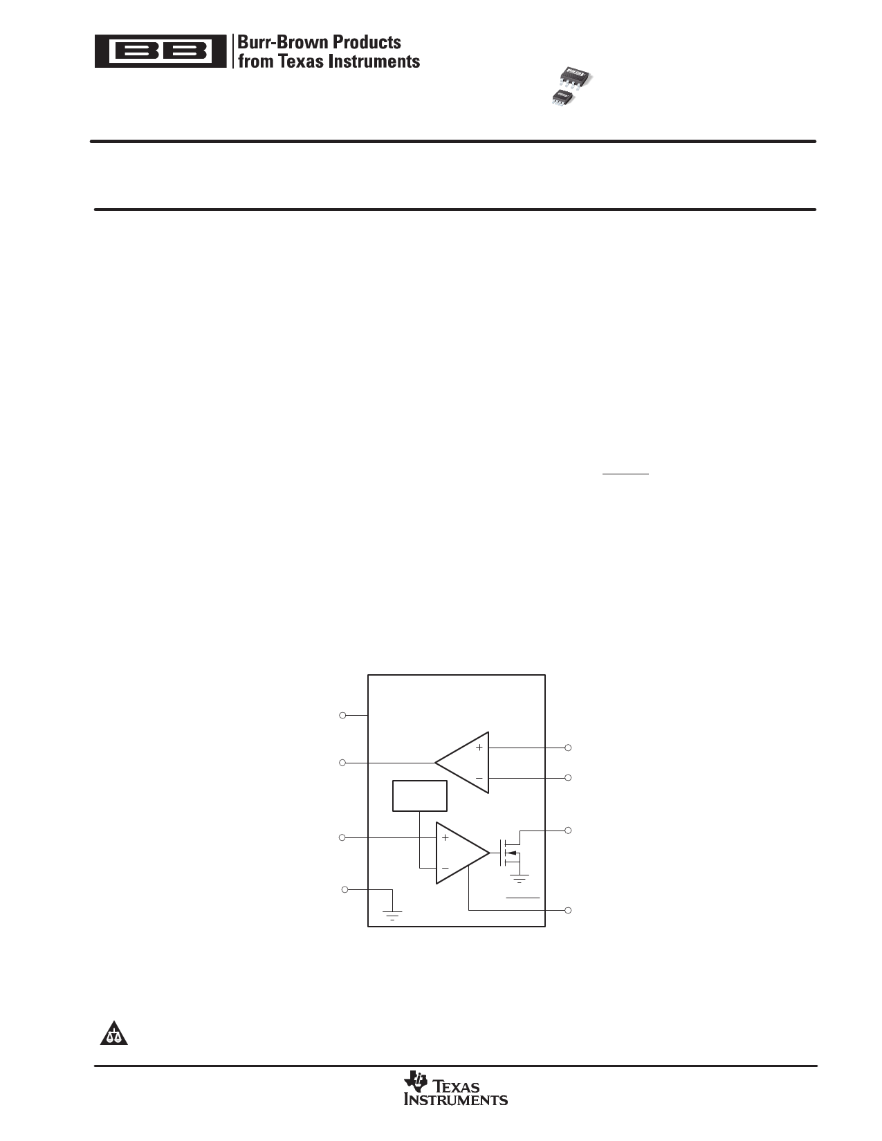
1
V+
INA200 (G = 20)
INA201 (G = 50)
INA202 (G = 100)
2 OUT
G
0.6V
Reference
3 CMPIN
VIN+ 8
VIN− 7
CMPOUT 6
Comparator
4 GND
RESET 5
Please be aware that an important notice concerning availability, standard warranty, and use in critical applications of Texas Instruments
semiconductor products and disclaimers thereto appears at the end of this data sheet.
All trademarks are the property of their respective owners.
PRODUCTION DATA information is current as of publication date. Products
conform to specifications per the terms of Texas Instruments standard warranty.
Production processing does not necessarily include testing of all parameters.
Copyright 2006, Texas Instruments Incorporated
www.ti.com
1 page 
www.ti.com
INA200
INA201
INA202
SBOS374 − NOVEMBER 2006
ELECTRICAL CHARACTERISTICS: GENERAL
Boldface limits apply over the specified temperature range: TA = −40°C to +125°C.
At TA = +25°C, VS = +12V, VCM = +12V, VSENSE = 100mV, RL = 10kΩ to GND, RPULL-UP = 5.1kΩ connected from CMPOUT to VS, and CMPIN = 1V,
unless otherwise noted.
INA200, INA201, INA202
GENERAL PARAMETERS
CONDITIONS
MIN
TYP
MAX
UNITS
POWER SUPPLY
Operating Power Supply
Quiescent Current
Over Temperature
Comparator Power-On Reset Threshold(1)
VS
IQ
VOUT = 2V
VSENSE = 0mV
+2.7
1350
1.5
+18
1800
1850
V
µA
µA
V
TEMPERATURE
Specified Temperature Range
Operating Temperature Range
Storage Temperature Range
Thermal Resistance
MSOP-8 Surface-Mount
SO-8
qJA
−40
+125
°C
−55
+150
°C
−65
+150
°C
200 °C/W
150 °C/W
(1) The INA200, INA201, and INA202 are designed to power-up with the comparator in a defined reset state as long as RESET is open or grounded. The comparator
is in reset as long as the power supply is below the voltage shown here. The comparator assumes a state based on the comparator input above this supply voltage.
If RESET is high at power-up, the comparator output comes up high and requires a reset to assume a low state, if appropriate.
5
5 Page 
www.ti.com
In the Typical Characteristics, the Output Error vs
Common-Mode Voltage curve shows the highest
accuracy for the this region of operation. In this plot,
VS = 12V; for VCM ≥ 12V, the output error is at its minimum.
This case is also used to create the VSENSE ≥ 20mV output
specifications in the Electrical Characteristics table.
Normal Case 2: VSENSE ≥ 20mV, VCM < VS
This region of operation has slightly less accuracy than
Normal Case 1 as a result of the common-mode operating
area in which the part functions, as seen in the Output Error
vs Common-Mode Voltage curve. As noted, for this graph
VS = 12V; for VCM < 12V, the Output Error increases as VCM
becomes less than 12V, with a typical maximum error of
0.005% at the most negative VCM = −16V.
Low VSENSE Case 1:
VSENSE < 20mV, −16V ≤ VCM < 0; and
Low VSENSE Case 3:
VSENSE < 20mV, VS < VCM ≤ 80V
Although the INA200 family of devices are not designed for
accurate operation in either of these regions, some
applications are exposed to these conditions. For
example, when monitoring power supplies that are
switched on and off while VS is still applied to the INA200,
INA201, or INA202, it is important to know what the
behavior of the devices will be in these regions.
As VSENSE approaches 0mV, in these VCM regions, the
device output accuracy degrades. A larger-than-normal
offset can appear at the current shunt monitor output with
a typical maximum value of VOUT = 300mV for
VSENSE = 0mV. As VSENSE approaches 20mV, VOUT
returns to the expected output value with accuracy as
specified in the Electrical Characteristics. Figure 3
illustrates this effect using the INA202 (Gain = 100).
2.0
1.8
1.6
1.4
1.2 Actual
1.0
0.8
Ideal
0.6
0.4
0.2
0
0 2 4 6 8 10 12 14 16 18 20
VSENSE (mV)
Figure 3. Example for Low VSENSE Cases 1 and 3
(INA202, Gain = 100)
Low VSENSE Case 2: VSENSE < 20mV, 0V ≤ VCM ≤ VS
This region of operation is the least accurate for the
INA200 family. To achieve the wide input common-mode
voltage range, these devices use two op amp front ends in
INA200
INA201
INA202
SBOS374 − NOVEMBER 2006
parallel. One op amp front end operates in the positive
input common-mode voltage range, and the other in the
negative input region. For this case, neither of these two
internal amplifiers dominates and overall loop gain is very
low. Within this region, VOUT approaches voltages close to
linear operation levels for Normal Case 2. This deviation
from linear operation becomes greatest the closer VSENSE
approaches 0V. Within this region, as VSENSE approaches
20mV, device operation is closer to that described by
Normal Case 2. Figure 4 illustrates this behavior for the
INA202. The VOUT maximum peak for this case is tested
by maintaining a constant VS, setting VSENSE = 0mV and
sweeping VCM from 0V to VS. The exact VCM at which VOUT
peaks during this test varies from part to part, but the VOUT
maximum peak is tested to be less than the specified VOUT
tested limit.
2.4
2.2
INA202 VOUT Tested Limit(1)
2.0
1.8
1.6
VCM2
VCM1
Ideal
1.4
1.2 VCM3
1.0
0.8
0.6
0.4
0.2
0
0
VCM4
24
VOUT tested limit at
VSENSE = 0mV, 0 ≤ VCM1 ≤ VS.
VCM2, VCM3, and VCM4 illustrate the variance
from part to part of the VCM that can cause
maximum VOUT with VSENSE < 20mV.
6 8 10 12 14 16 18 20 22 24
VSENSE (mV)
NOTE: (1) INA200 VOUT Tested Limit = 0.4V. INA201 VOUT Tested Limit = 1V.
Figure 4. Example for Low VSENSE Case 2
(INA202, Gain = 100)
SELECTING RS
The value chosen for the shunt resistor, RS, depends on
the application and is a compromise between small-signal
accuracy and maximum permissible voltage loss in the
measurement line. High values of RS provide better
accuracy at lower currents by minimizing the effects of
offset, while low values of RS minimize voltage loss in the
supply line. For most applications, best performance is
attained with an RS value that provides a full-scale shunt
voltage range of 50mV to 100mV. Maximum input voltage
for accurate measurements is 500mV.
TRANSIENT PROTECTION
The −16V to +80V common-mode range of the INA200,
INA201, and INA202 is ideal for withstanding automotive
fault conditions ranging from 12V battery reversal up to
+80V transients, since no additional protective
components are needed up to those levels. In the event
that the INA200, INA201, and INA202 are exposed to
transients on the inputs in excess of their ratings, then
external transient absorption with semiconductor transient
absorbers (such as zeners) will be necessary. Use of
11
11 Page | ||
| Páginas | Total 19 Páginas | |
| PDF Descargar | [ Datasheet INA202.PDF ] | |
Hoja de datos destacado
| Número de pieza | Descripción | Fabricantes |
| INA200 | High-Side Measurement Current-Shunt Monitor | Texas Instruments |
| INA200 | (INA200 - INA202) High-Side Measurement Current-Shunt Monitor | Burr-Brown |
| INA200-Q1 | INA20x-Q1 Automotive Grade 16-V to +80-V Low- or High-Side High-Speed Voltage-Output Current-Sense Amplifier With Comparator and Reference (Rev. C) | Texas Instruments |
| INA201 | (INA200 - INA202) High-Side Measurement Current-Shunt Monitor | Burr-Brown |
| Número de pieza | Descripción | Fabricantes |
| SLA6805M | High Voltage 3 phase Motor Driver IC. |
Sanken |
| SDC1742 | 12- and 14-Bit Hybrid Synchro / Resolver-to-Digital Converters. |
Analog Devices |
|
DataSheet.es es una pagina web que funciona como un repositorio de manuales o hoja de datos de muchos de los productos más populares, |
| DataSheet.es | 2020 | Privacy Policy | Contacto | Buscar |