|
|
|
PDF NCP5030 Data sheet ( Hoja de datos )
| Número de pieza | NCP5030 | |
| Descripción | Buck Boost Converter to Drive a Single LED | |
| Fabricantes | ON Semiconductor | |
| Logotipo | ||
Hay una vista previa y un enlace de descarga de NCP5030 (archivo pdf) en la parte inferior de esta página. Total 14 Páginas | ||
|
No Preview Available !
www.DataSheet4U.com
NCP5030
Product Preview
Buck−Boost Converter
to Drive a Single LED from 1
Li−Ion or 3 Alkaline
Batteries
The NCP5030 is a fixed frequency PWM buck−boost converter
optimized for constant current applications such as driving
high−powered white LED. The buck−boost is implemented in an
H−bridge topology and has an adaptive architecture where it operates
in one of three modes: boost, buck−boost, or buck depending on the
input and output voltage condition. This device has been designed
with high−efficiency for use in portable applications and is capable
of driving in DC up to 900 mA into a high power LED for flashlight /
torch applications. To protect the device cycle−by−cycle current
limiting and a thermal shutdown circuit have been incorporated as
well as output over−voltage protection. The 700 kHz switching
frequency allows the use of a low value 4.7 mH and ceramic
capacitors. The NCP5030 is housed in a low profile space efficient
3x4 mm thermally enhanced WDFN.
Features
• Efficiency: 87% at 500 mA and 3.3 V VIN
• Internal Synchronous Rectifier, No Schottky Diodes
• Adjustable Switching Limit Current to Optimize inductor size
• 0.3 mA Shut−down Control with “True−Cut off”
• Input Voltage Range from 2.7 V to 5.5 V
• 200 mV Feedback Voltage
• Output Over−voltage and Thermal Shut Down Protection
Typical Applications
• Portable Flashlight / Torch Lights
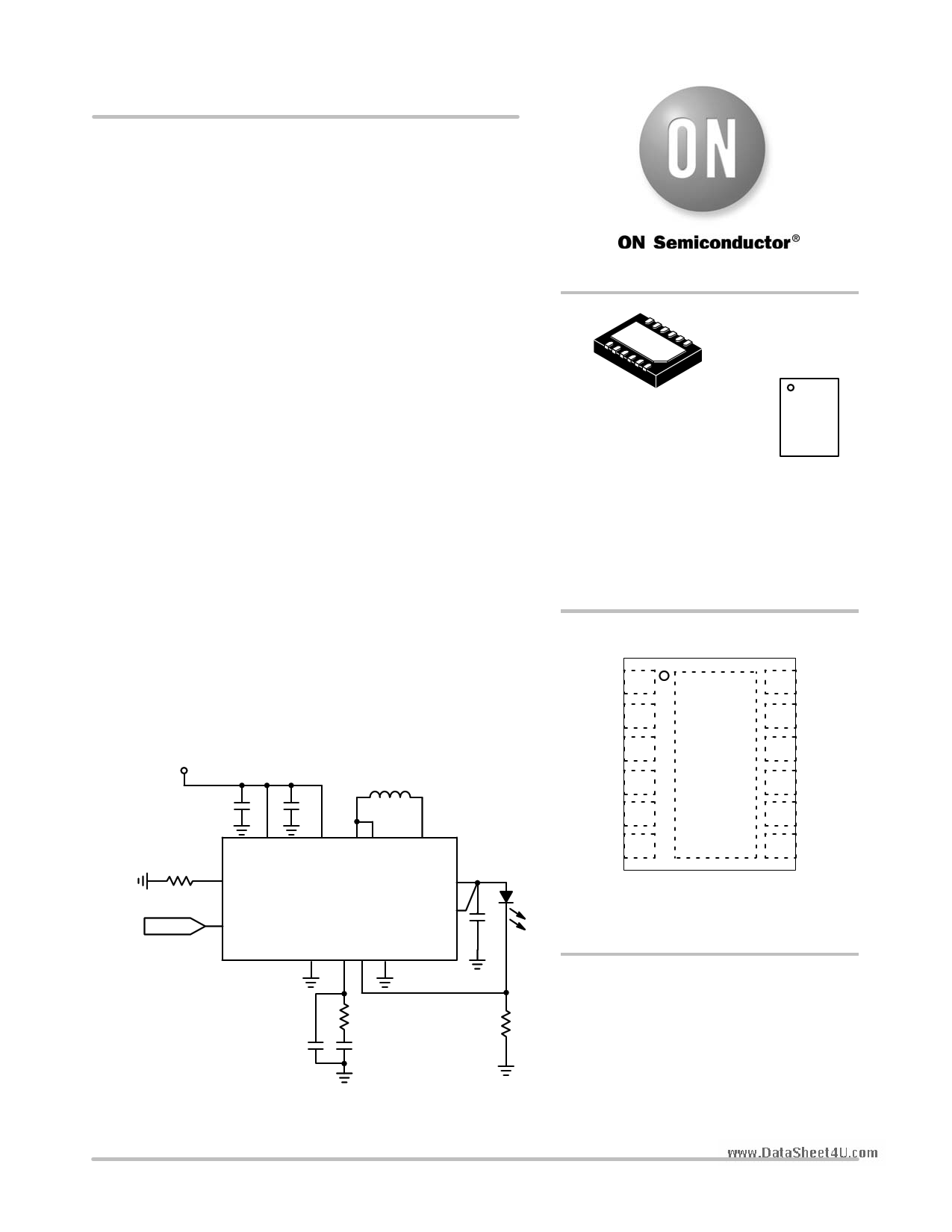
Vin
1 Cell
Cin
Li−Ion
1 mF
2.7 to 5.5
C2
10 mF
Cin
4.7 mH
L1
39 k
R1
ENABLE
PCA
CTRL
VOUT
C3
22 mF
D1
VS
NCP5030
Cout
L1: TDK RLF7030T−4R7M3R4
C1: 1 mF 6.3 V X5R
C2: 10 mF 3.6 V 0805
TDK: C2012X5R0J106MT
C3: 22 mF 6.3 V X5R
TDK: C2012X5R0J226MTJ
C4
22 pF
R2
100 k
C5
330 pF
R3
220 m
RSENSE
Figure 1. Typical Application Circuit
This document contains information on a product under development. ON Semiconductor
reserves the right to change or discontinue this product without notice.
© Semiconductor Components Industries, LLC, 2006
November, 2006 − Rev. P1
1
http://onsemi.com
12 MARKING
DIAGRAM
11
WDFN12 3x4
MT SUFFIX
CASE 506AY
5030
ALYWG
G
5030 = Specific Device Code
A = Assembly Location
L = Wafer Lot
Y = Year
W = Work Week
G = Pb−Free Package
(Note: Microdot may be in either location)
PIN CONNECTIONS
FB 1
COMP 2
CTRL 3
PVIN 4
LX1 5
LX1 6
12 PCA
11 AGND
10 VIN
13
9 VS
8 VOUT
7 LX2
(Top View)
Exposed pad (Pin 13) is PGND
must be soldered to PCB GND plane
ORDERING INFORMATION
See detailed ordering and shipping information in the package
dimensions section on page 13 of this data sheet.
Publication Order Number:
NCP5030/D
1 page 
www.DataSheet4U.com
NCP5030
ELECTRICAL CHARACTERISTICS (Limits apply for TA between −40°C to +85°C and Vin = 3.6 V unless otherwise noted.)
Characteristic
Symbol Min Typ Max
Operational Power Supply
VIN 2.7 − 5.5
Maximum Inductor Current (Note 11) (See Figure 8)
IPEAK_MAX
−20%
4.0
+20%
Switches P1 and P2 ON Resistance
PMOS RDSON
−
100
−
Switches N1 and N2 ON Resistance
NMOS RDSON
−
100
−
Switches P1 and P2 Leakage Current
PMOS L − 0.5 −
Switches N1 and N2 Leakage Current
NMOS L − 0.5 −
Internal Oscillator Frequency (Note 8)
FOSC
600 700 800
Efficiency (Notes 9, 10 and 11)
EFF − 85 −
Output Voltage Range (Note 11)
VOUT 2.2 − 5.5
VOUT−VIN Threshold to Change Mode from Boost to Buck−Boost
TBOOST − 375 −
VIN−VOUT Threshold to Change Mode from Buck−Boost to Buck
TBUCK
− 650 −
Threshold to Change Mode Hysteresis
HMODE
− 100 −
Available Output Power (Note 11)
When Vin ≥ 3.1 V (Vout = 4.7 V, 900 mA)
POUT
4.3 −
−
Feedback Voltage Threshold in Steady State at 25°C
FBV 190 200 210
Line Regulation, Measured on FB Pin (Note 8)
From DC to 100 Hz and RFB = 1 W
FBVLR
− 5.0 −
Feedback Input Current
FBC − − 0.1
Standby Current at IOUT = 0 mA, CTRL = Low, Vbat = 4.2 V
ISTB − 0.3 3.0
Quiescent Current Switching at IOUT = 0 mA, CTRL = High, Vbat = 4.2 V
(Note 12)
IQS
− 5.0 −
VIN Undervoltage Lockout
Threshold to Enable the Converter
UVLO
2.2 2.4 2.6
Undervoltage Lockout Hysteresis
UVLOH
−
Soft−start Time (Note 11)
SST −
Limit of CTRL pin PWM Dimming Frequency (Note 11)
FDIM
−
Thermal Shutdown Protection
TSD −
Thermal Shutdown Protection Hysteresis
TSDH
−
Voltage Input Logic Low
VIL −
Voltage Input Logic High
VIH 1.2
CTRL Pin Pulldown Resistance
RCTRL
150
8. TA between −10°C to +85°C
9. Efficiency is defined by 100 * (Pout/Pin) at 25°C. Vin = 3.3 V, IOUT = 500 mA, Load = 1 LED (Vf = 3.9 V)
10. L = 4.7 mH (TDK RLF7030T−4R7M3R4), Cout = 22 mF X5R
11. Guaranteed by design and characterized.
12. The overall tolerance is dependent on the accuracy of the external resistor.
100
1000
0.2
160
20
−
−
220
−
−
−
−
−
0.4
−
290
Unit
V
A
mW
mW
mA
mA
MHz
%
V
mV
mV
mV
W
mV
mV/V
mA
mA
mA
V
mV
ms
kHz
°C
°C
V
V
kW
http://onsemi.com
5
5 Page 
www.DataSheet4U.com
NCP5030
Current Selection
Figure 22 shows an application schematic to drive two
selected currents I1 and I2.
ILED + I1 ) I2
(eq. 2)
VOUT
LED
VS
NCP5030
200 mV
FLASH/TORCH
NTHS5404
RSENSE
R2 R1
I2 I1
M1
Figure 22. Two Current Selections
Low level active logic on gate of M1 enables the low
current mode, So I2 = 0 and I1 = ILED = 200 mV / R1. For
example, should one need 200 mA for low current mode
and 800 mA for high current mode, R1 should be selected
according to the following below:
R1
+
FBV
I1
+
200
200
mV
mA
+
1.0
W
(eq. 3)
So an active high logic level on gate of M1 enables the
high current mode then IFLASH = I1 + I2 and according
Equation 2 and 3, R2 should be selected regarding the
following equation:
R2
+
FBV
IFLASH *
I1
*
RDSON_M1
R2
+
800
200 mV
mA * 200
mA
*
33
mW
(eq. 4)
R2 + 300 mW
The following resistors are recommended, but are not
limited to:
PANASONIC ERJ3BQF1R0V (1.0 W 1% 0603)
PANASONIC ERJ3BQFR30V (300 mW 1% 0603)
PANASONIC ERJ3BQJ1R0V (1.0 W 5% 0603)
PANASONIC ERJ3BQJR30V (300 mW 5% 0603)
Analogue Dimming
In white LED applications, it is desirable to operate the
LEDs at a specific operating current, to prevent color shift
as a function of bias current. As a consequence, it is
recommended to dim the LED current by Pulse Width
Modulation techniques. A low frequency PWM signal can
be applied to the CTRL input. LED brightness can be
changed by varying the duty cycle. To avoid any optical
flicker the frequency must be higher than 100 Hz and
preferably less than 300 Hz. Because of the soft−start
function set at 1000 ms (nominal), higher frequency would
cause the device to remain active with lower than expected
brightness. Nevertheless, in this case a dimming control
using a filtered PWM signal can be used. In addition, for
DC voltage control the same technique is suitable and the
filter is taken away. Please refer to “NPC5030 Dimming
Control Application Note”.
Inductor Selection
Three main electrical parameters need to be considered
when choosing an inductor: the value of the inductor, the
saturation current and the DCR. Firstly, we need to check
if the inductor is able to handle the peak current without
saturating. Therefore, we have to consider that the
maximum peak inductor current is in Buck−Boost mode
when VOUT is closed TBOOST threshold for the lower
operating VIN. Obviously, the peak current inductor is
higher when this device supplies the maximum required
current. In this case, the DC−DC converter is supposed to
operate in Continuous Conduction Mode (CCM). The
dotted curve in Figure 23 gives the inductor peak current
as a function of load current:
2.5
2 Switch Current Limit
Setup by RPCA
1.5
1
Operating Inductor Peak Current
0.5
0
100 200 300 400 500 600 700 800 900
Iout (mA)
Figure 23. Inductor Peak Currents Vs. IOUT (mA)
Finally, an acceptable DCR must be selected regarding
losses in the coil and must be lower than 100 mW to limit
excessive voltage drop. In addition, as DCR is reduced,
overall efficiency will improve. Some recommended
inductors are included but are not limited to:
TDK VLF5014AT−4R71R1
TDK RLF7030−4R7M3R4
COPPER BUSSMANN FP3−4R7
MURATA LQH43CN4R7M03L
NIC: TBD
Switch Current Limit
This safety feature is clamping the maximum allowed
current in the inductor according to external RPCA resistor,
which is connected between PCA input and the ground.
http://onsemi.com
11
11 Page | ||
| Páginas | Total 14 Páginas | |
| PDF Descargar | [ Datasheet NCP5030.PDF ] | |
Hoja de datos destacado
| Número de pieza | Descripción | Fabricantes |
| NCP5030 | Buck Boost Converter to Drive a Single LED | ON Semiconductor |
| Número de pieza | Descripción | Fabricantes |
| SLA6805M | High Voltage 3 phase Motor Driver IC. |
Sanken |
| SDC1742 | 12- and 14-Bit Hybrid Synchro / Resolver-to-Digital Converters. |
Analog Devices |
|
DataSheet.es es una pagina web que funciona como un repositorio de manuales o hoja de datos de muchos de los productos más populares, |
| DataSheet.es | 2020 | Privacy Policy | Contacto | Buscar |