|
|
|
PDF PDU10256H Data sheet ( Hoja de datos )
| Número de pieza | PDU10256H | |
| Descripción | ECL-INTERFACED PROGRAMMABLE DELAY LINE | |
| Fabricantes | Data Delay Devices | |
| Logotipo | ||
Hay una vista previa y un enlace de descarga de PDU10256H (archivo pdf) en la parte inferior de esta página. Total 5 Páginas | ||
|
No Preview Available !
www.DataSheet4U.com
8-BIT, ECL-INTERFACED
PROGRAMMABLE DELAY LINE
(SERIES PDU10256H)
PDU10256H
data
delay
3
®
devices, inc.
FEATURES
• Digitally programmable in 128 delay steps
• Monotonic delay-versus-address variation
• Precise and stable delays
• Input & outputs fully 10KH-ECL interfaced & buffered
• Fits 48-pin DIP socket
PIN DESCRIPTIONS
IN Signal Input
OUT Signal Output
A0-A7 Address Bits
ENB Output Enable
VEE -5 Volts
GND Ground
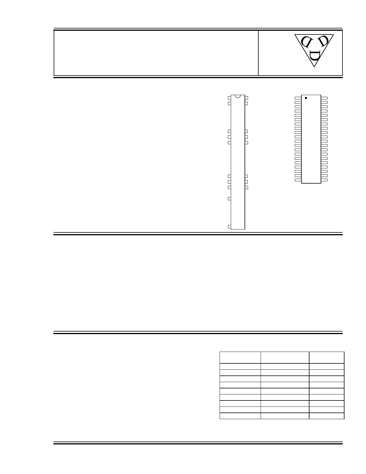
PACKAGES
GND 1 48 GND
ENB 2 47 OUT
A0 7 42 A1
VEE 8 41 A2
GND 9 40 GND
A3
VEE
15 34 A4
16 33 A5
N/C
N/C
OUT
GND
ENB
N/C
N/C
N/C
GND
ENB
N/C
N/C
N/C
N/C
N/C
N/C
N/C
GND
ENB
IN
1 40
2 39
3 38
4 37
5 36
6 35
7 34
8 33
9 32
10 31
11 30
12 29
13 28
14 27
15 26
16 25
17 24
18 23
19 22
20 21
N/C
N/C
A2
A1
VEE
A0
N/C
A5
A4
VEE
A3
N/C
N/C
N/C
N/C
N/C
N/C
A7
VEE
A6
GND 17 32 GND
IN 19
PDU10256H-xxC5 SMD
PDU10256H-xxMC5 Mil SMD
PDU10256H-xx DIP
A6 23
PDU10256H-xxM Mil DIP
VEE 24 25 A7
FUNCTIONAL DESCRIPTION
The PDU10256H-series device is an 8-bit digitally programmable delay line. The delay, TDA, from the
input pin (IN) to the output pin (OUT) depends on the address code (A7-A0) according to the following
formula:
TDA = TD0 + TINC * A
where A is the address code, TINC is the incremental delay of the device, and TD0 is the inherent delay of
the device. The incremental delay is specified by the dash number of the device and can range from
0.5ns through 10ns, inclusively. The enable pin (ENB) is held LOW during normal operation. When this
signal is brought HIGH, OUT is forced into a LOW state. The address is not latched and must remain
asserted during normal operation.
SERIES SPECIFICATIONS
• Total programmed delay tolerance: 5% or 2ns,
whichever is greater
Inherent delay (TD0): 12ns typical
• Setup time and propagation delay:
Address to input setup (TAIS): 3.6ns
Disable to output delay (TDISO): 1.7ns typical
• Operating temperature: 0° to 70° C
• Temperature coefficient: 100PPM/°C (excludes TD0)
• Supply voltage VEE: -5VDC ± 5%
• Power Dissipation: 925mw typical (no load)
• Minimum pulse width: 16% of total delay
©1997 Data Delay Devices
DASH NUMBER SPECIFICATIONS
Part
Number
PDU10256H-.5
PDU10256H-1
PDU10256H-2
PDU10256H-3
PDU10256H-4
PDU10256H-5
PDU10256H-6
PDU10256H-8
PDU10256H-10
Incremental Delay
Per Step (ns)
0.5 ± 0.3
1.0 ± 0.5
2.0 ± 0.5
3.0 ± 1.0
4.0 ± 1.0
5.0 ± 1.5
6.0 ± 1.5
8.0 ± 2.0
10.0 ± 2.0
Total
Delay (ns)
127.5 ± 6.4
255 ± 12.8
510 ± 25.5
765 ± 38.2
1020 ± 51.0
1275 ± 63.8
1530 ± 76.5
2040 ± 102
2550 ± 128
NOTE: Any dash number between .5 and 10
not shown is also available.
Doc #97047
12/17/97
DATA DELAY DEVICES, INC.
3 Mt. Prospect Ave. Clifton, NJ 07013
1
1 page 
DELAY LINE AUTOMATED TESTING
PDU10256H
TEST CONDITIONS
INPUT:
Ambient Temperature: 25oC ± 3oC
Supply Voltage (Vcc): -5.0V ± 0.1V
Input Pulse:
Standard 10KH ECL
levels
Source Impedance: 50Ω Max.
Rise/Fall Time:
2.0 ns Max. (measured
between 20% and 80%)
Pulse Width:
Period:
PWIN = 1.5 x Total Delay
PERIN = 10 x Total Delay
OUTPUT:
Load:
Cload:
Threshold:
50Ω to -2V
5pf ± 10%
(VOH + VOL) / 2
(Rising & Falling)
NOTE: The above conditions are for test only and do not in any way restrict the operation of the device.
PULSE
GENERATOR
OUT
TRIG
IN DEVICE UNDER OUT
TEST (DUT)
REF
IN
TRIG
OSCILLOSCOPE
ADDRESS SELECT
Test Setup
INPUT
SIGNAL
OUTPUT
SIGNAL
TRISE
PWIN
PERIN
TFALL
80% VIH 80%
50%
50%
20% 20%
VIL
TRISE
TFALL
50%
VOH
50%
Timing Diagram For Testing
VOL
Doc #97047
12/17/97
DATA DELAY DEVICES, INC.
3 Mt. Prospect Ave. Clifton, NJ 07013
5
5 Page | ||
| Páginas | Total 5 Páginas | |
| PDF Descargar | [ Datasheet PDU10256H.PDF ] | |
Hoja de datos destacado
| Número de pieza | Descripción | Fabricantes |
| PDU10256H | ECL-INTERFACED PROGRAMMABLE DELAY LINE | Data Delay Devices |
| Número de pieza | Descripción | Fabricantes |
| SLA6805M | High Voltage 3 phase Motor Driver IC. |
Sanken |
| SDC1742 | 12- and 14-Bit Hybrid Synchro / Resolver-to-Digital Converters. |
Analog Devices |
|
DataSheet.es es una pagina web que funciona como un repositorio de manuales o hoja de datos de muchos de los productos más populares, |
| DataSheet.es | 2020 | Privacy Policy | Contacto | Buscar |