|
|
|
PDF ADM2483 Data sheet ( Hoja de datos )
| Número de pieza | ADM2483 | |
| Descripción | Half-Duplex iCoupler Isolated RS-485 Transceiver | |
| Fabricantes | Analog Devices | |
| Logotipo | ||
Hay una vista previa y un enlace de descarga de ADM2483 (archivo pdf) en la parte inferior de esta página. Total 18 Páginas | ||
|
No Preview Available !
Data Sheet
FEATURES
RS-485 transceiver with electrical data isolation
Complies with ANSI TIA/EIA RS-485-A and ISO 8482: 1987(E)
500 kbps data rate
Slew rate-limited driver outputs
Low power operation: 2.5 mA max
Suitable for 5 V or 3 V operations (VDD1)
High common-mode transient immunity: >25 kV/μs
True fail-safe receiver inputs
Chatter-free power-up/power-down protection
256 nodes on bus
Thermal shutdown protection
Safety and regulatory approvals
UL recognition: 2500 V rms for 1 minute per UL 1577
CSA Component Acceptance Notice 5A
IEC 609501 800 V rms (basic), 400 V rms (reinforced)
VDE Certificate of Conformity
DIN V VDE V 0884-10 (VDE V 0884-10): 2006-12
VIORM = 560 V peak
CQC certification per GB4943.1-2011
Operating temperature range: −40°C to +85°C
APPLICATIONS
Low power RS-485/RS-422 networks
Isolated interfaces
Building control networks
Multipoint data transmission systems
GENERAL DESCRIPTION
The ADM2483 differential bus transceiver is an integrated,
galvanically isolated component designed for bidirectional data
communication on balanced, multipoint bus transmission lines.
It complies with ANSI EIA/TIA-485-A and ISO 8482: 1987(E).
Using Analog Devices’ iCoupler technology, the ADM2483
combines a 3-channel isolator, a three-state differential line
driver, and a differential input receiver into a single package.
The logic side of the device is powered with either a 5 V or 3 V
supply, and the bus side uses a 5 V supply only.
The ADM2483 is slew-limited to reduce reflections with
improperly terminated transmission lines. The controlled slew
rate limits the data rate to 500 kbps. The device’s input impedance
is 96 kΩ, allowing up to 256 transceivers on the bus. Its driver
has an active-high enable feature. The driver differential outputs
Half-Duplex, iCoupler®
Isolated RS-485 Transceiver
ADM2483
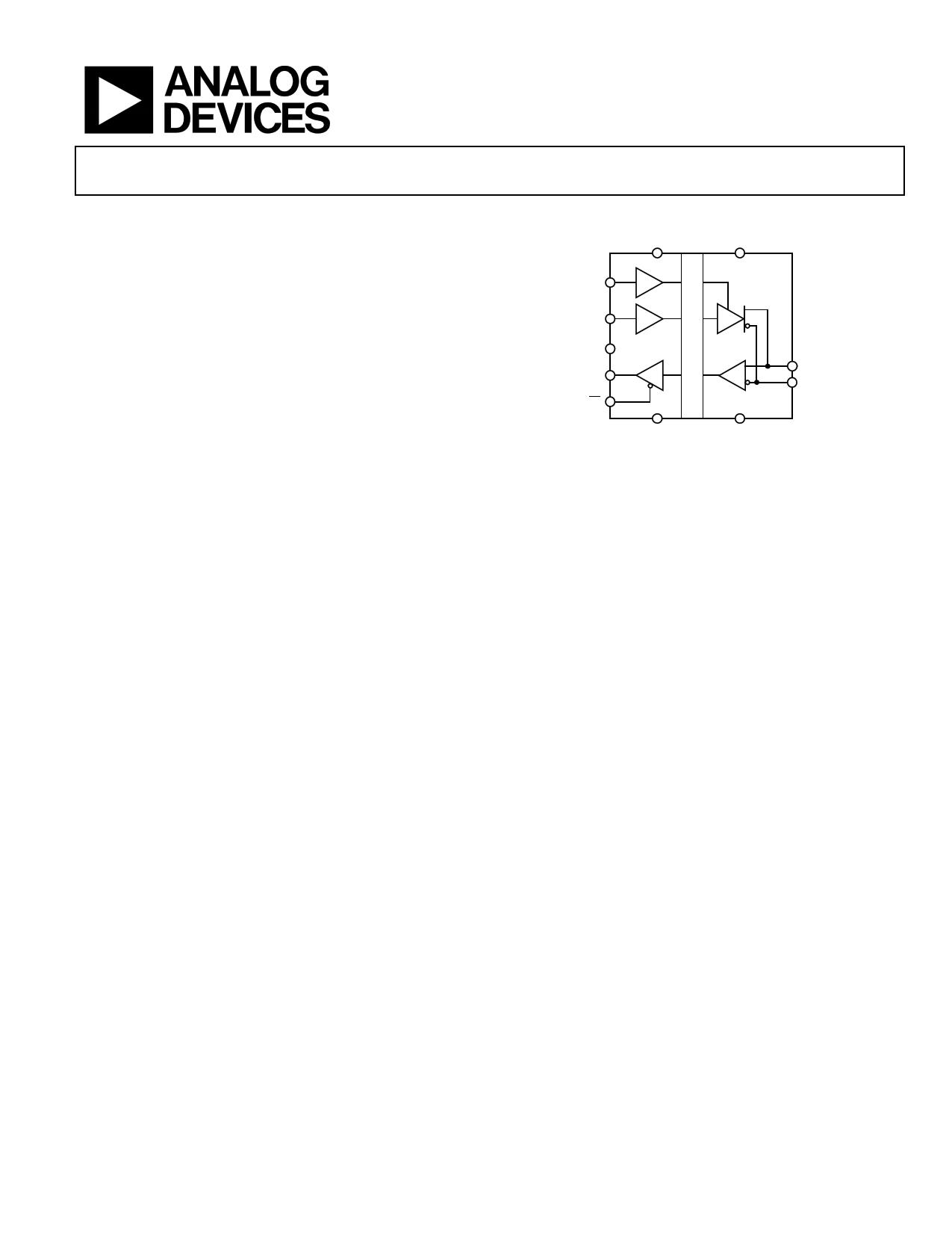
FUNCTIONAL BLOCK DIAGRAM
VDD1
VDD2
ADM2483
DE
TxD
PV
RxD
RE
GND1
GND2
Figure 1.
A
B
and receiver differential inputs are connected internally to form
a differential I/O port. When the driver is disabled or when
VDD1 or VDD2 = 0 V, this imposes minimal loading on the bus.
An active-high receiver disable feature, which causes the receive
output to enter a high impedance state, is provided as well.
The receiver inputs have a true fail-safe feature that ensures a
logic-high receiver output level when the inputs are open or
shorted. This guarantees that the receiver outputs are in a
known state before communication begins and at the point
when communication ends.
Current limiting and thermal shutdown features protect against
output short circuits and bus contention situations that might
cause excessive power dissipation. The part is fully specified
over the industrial temperature range and is available in a
16-lead, wide body SOIC package.
Rev. E
Document Feedback
Information furnished by Analog Devices is believed to be accurate and reliable. However, no
responsibility is assumed by Analog Devices for its use, nor for any infringements of patents or other
rights of third parties that may result from its use. Specifications subject to change without notice. No
license is granted by implication or otherwise under any patent or patent rights of Analog Devices.
Trademarksandregisteredtrademarksarethepropertyoftheirrespectiveowners.
One Technology Way, P.O. Box 9106, Norwood, MA 02062-9106, U.S.A.
Tel: 781.329.4700 ©2004–2016 Analog Devices, Inc. All rights reserved.
Technical Support
www.analog.com
1 page 
Data Sheet
ABSOLUTE MAXIMUM RATINGS
TA = 25°C, unless otherwise noted. All voltages are relative to
their respective ground.
Table 3.
Parameter
VDD1
VDD2
Digital Input Voltage (DE, RE, TxD)
Digital Output Voltage
RxD
Driver Output/Receiver Input Voltage
ESD Rating: Contact (Human Body
Model) (A, B Pins)
Operating Temperature Range
Storage Temperature Range
Average Output Current per Pin
θJA Thermal Impedance
Lead Temperature
Soldering (10 sec)
Vapor Phase (60 sec)
Infrared (15 sec)
Rating
−0.5 V to +7 V
−0.5 V to +6 V
−0.5 V to VDD1 + 0.5 V
−0.5 V to VDD1 + 0.5 V
−9 V to +14 V
±2 kV
−40°C to +85°C
−55°C to +150°C
−35 mA to +35 mA
73°C/W
260°C
215°C
220°C
Stresses at or above those listed under Absolute Maximum
Ratings may cause permanent damage to the product. This is a
stress rating only; functional operation of the product at these
or any other conditions above those indicated in the operational
section of this specification is not implied. Operation beyond
the maximum operating conditions for extended periods may
affect product reliability.
ADM2483
Table 4. Maximum Continuous Working Voltage1
Parameter
Max Unit Reference Standard
AC Voltage
Bipolar Waveform
Basic Insulation 565 VPEAK 50-year minimum lifetime
Reinforced
Insulation
565 VPEAK 50-year minimum lifetime
Unipolar Waveform
Basic Insulation 1131 VPEAK 50-year minimum lifetime
Reinforced
Insulation
864 VPEAK Lifetime limited by
package creepage
maximum approved
working voltage per IEC
60950-1
DC Voltage
Basic Insulation
1066 VPEAK Lifetime limited by
package creepage
maximum approved
working voltage per IEC
60950-1
Reinforced
Insulation
529 VPEAK Lifetime limited by
package creepage
maximum approved
working voltage per IEC
60950-1
1 Refers to continuous voltage magnitude imposed across the isolation
barrier.
ESD CAUTION
Rev. D | Page 5 of 18
5 Page 
Data Sheet
TYPICAL PERFORMANCE CHARACTERISTICS
1.6
IDD1_RCVR_ENABLE @ 5.5V
1.4
1.2
1.0
0.8
IDD2_DE_ENABLE @ 5.5V
0.6
0.4
0.2
0
–40
25
85
TEMPERATURE (°C)
Figure 13. Unloaded Supply Current vs. Temperature
120
100
80
60
40
20
0
0 0.5 1.0 1.5 2.0 2.5 3.0 3.5 4.0 4.5 5.0
OUTPUT VOLTAGE (V)
Figure 14. Output Current vs. Driver Output Low Voltage
–10
–30
–50
–70
–90
–110
0
0.5 1.0 1.5 2.0 2.5 3.0 3.5 4.0 4.5 5.0
OUTPUT VOLTAGE (V)
Figure 15. Output Current vs. Driver Output High Voltage
ADM2483
0.32
0.30
0.28
0.26
0.24
0.22
0.20
–40 –25 –10
5
20 35 50 65 80
TEMPERATURE (°C)
Figure 16. Receiver Output Low Voltage vs. Temperature, I = –4mA
4.78
4.76
4.74
4.72
4.70
4.68
4.66
–40 –25 –10
5
20 35 50 65 80
TEMPERATURE (°C)
Figure 17. Receiver Output High Voltage vs. Temperature, I = 4 mA
90
80
70
60
50
40
30
20
10
0
0 0.5 1.0 1.5 2.0 2.5 3.0 3.5 4.0 4.5 5.0
DIFFERENTIAL OUTPUT VOLTAGE (V)
Figure 18. Driver Output Current vs. Differential Output Voltage
Rev. D | Page 11 of 18
11 Page | ||
| Páginas | Total 18 Páginas | |
| PDF Descargar | [ Datasheet ADM2483.PDF ] | |
Hoja de datos destacado
| Número de pieza | Descripción | Fabricantes |
| ADM2481 | Isolated RS-485 Transceiver | Analog Devices |
| ADM2482E | 2.5 kV Isolated RS-485 Transceivers | Analog Devices |
| ADM2483 | Half-Duplex iCoupler Isolated RS-485 Transceiver | Analog Devices |
| ADM2484E | Isolated RS-485 Transceiver | Analog Devices |
| Número de pieza | Descripción | Fabricantes |
| SLA6805M | High Voltage 3 phase Motor Driver IC. |
Sanken |
| SDC1742 | 12- and 14-Bit Hybrid Synchro / Resolver-to-Digital Converters. |
Analog Devices |
|
DataSheet.es es una pagina web que funciona como un repositorio de manuales o hoja de datos de muchos de los productos más populares, |
| DataSheet.es | 2020 | Privacy Policy | Contacto | Buscar |