|
|
|
PDF ADM3071E Data sheet ( Hoja de datos )
| Número de pieza | ADM3071E | |
| Descripción | (ADM3070E - ADM3078E) low power data transceivers | |
| Fabricantes | Analog Devices | |
| Logotipo | ||
Hay una vista previa y un enlace de descarga de ADM3071E (archivo pdf) en la parte inferior de esta página. Total 20 Páginas | ||
|
No Preview Available !
www.DataSheet4U.com
3.3 V, ±15 kV ESD-Protected, Half- and
Full-Duplex, RS-485/RS-422 Transceivers
ADM3070E/ADM3071E/ADM3072E/ADM3073E/ADM3074E/ADM3075E/ADM3076E/ADM3077E/ADM3078E
FEATURES
TIA/EIA RS-485/RS-422 compliant
±15 kV ESD protection on RS-485 input/output pins
Data rates
ADM3070E/ADM3071E/ADM3072E: 250 kbps
ADM3073E/ADM3074E/ADM3075E: 500 kbps
ADM3076E/ADM3077E/ADM3078E: 16 Mbps
Half- and full-duplex options
True fail-safe receiver inputs
Up to 256 nodes on the bus
−40°C to +125°C temperature option
Hot-swap input structure on DE and RE pins
Reduced slew rates for low EMI
Low power shutdown current (all except
ADM3071E/ADM3074E/ADM3077E)
Outputs high-Z when disabled or powered off
Common-mode input range: −7 V to +12 V
Thermal shutdown and short-circuit protection
8-lead and 14-lead narrow SOIC packages
APPLICATIONS
Power/energy metering
Industrial control
Lighting systems
Telecommunications
Security systems
Instrumentation
GENERAL DESCRIPTION
The ADM3070E to ADM3078E are 3.3 V, low power data
transceivers with ±15 kV ESD protection suitable for full- and
half-duplex communication on multipoint bus transmission
lines. They are designed for balanced data transmission, and they
comply with TIA/EIA standards RS-485 and RS-422.
The devices have an ⅛ unit load receiver input impedance,
which allows up to 256 transceivers on a bus. Because only one
driver should be enabled at any time, the output of a disabled or
powered-down driver is tristated to avoid overloading the bus.
The receiver inputs have a true fail-safe feature, which
eliminates the need for external bias resistors and ensures a
logic high output level when the inputs are open or shorted.
This guarantees that the receiver outputs are in a known state
before communication begins and when communication ceases.
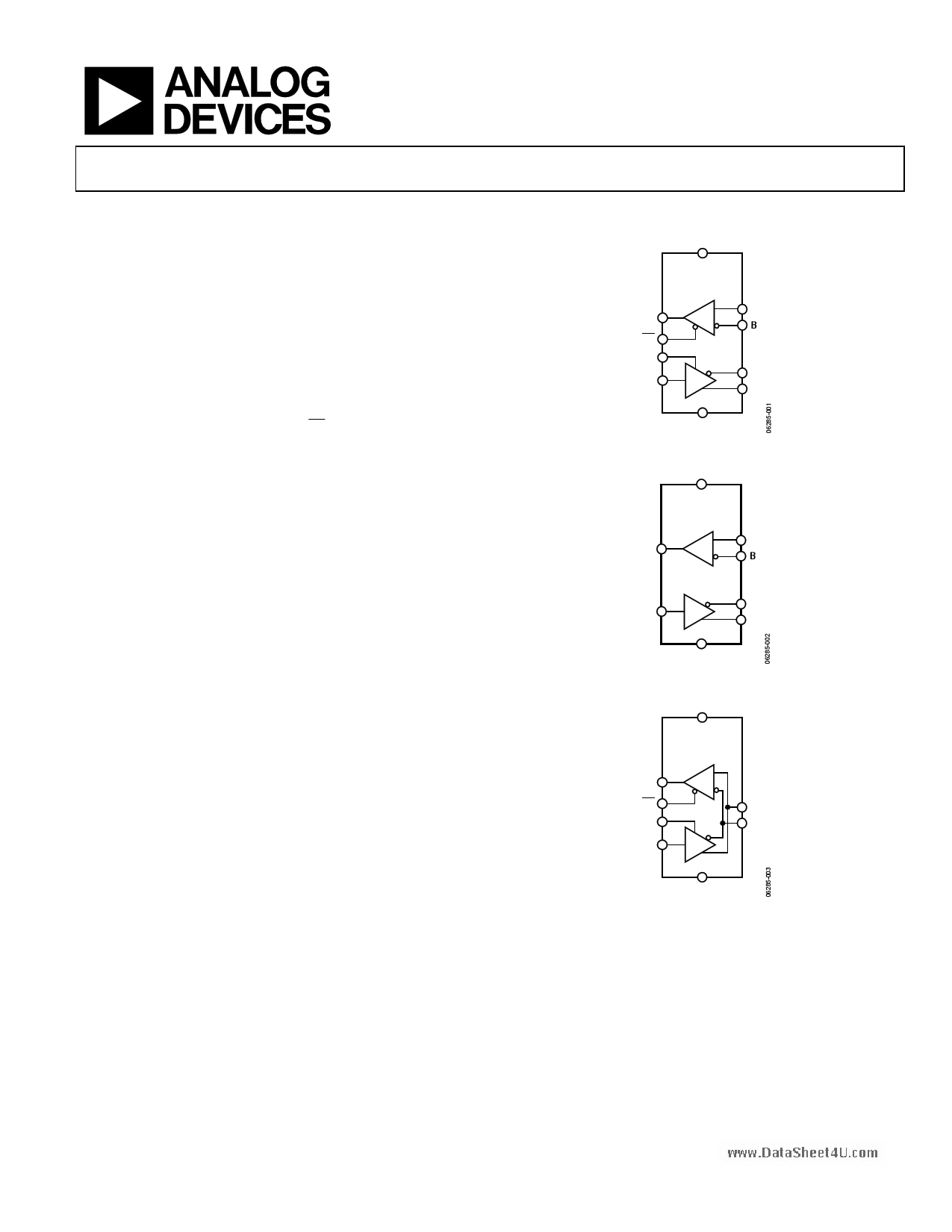
FUNCTIONAL BLOCK DIAGRAMS
VCC
ADM3070E/
ADM3073E/
ADM3076E
RO R
RE
DE
DI D
A
B
Z
Y
GND
Figure 1.
VCC
ADM3071E/
ADM3074E/
ADM3077E
A
RO R B
DI D
Z
Y
GND
Figure 2.
VCC
ADM3072E/
ADM3075E/
ADM3078E
.
RO R
RE
DE
DI D
A
B
GND
Figure 3.
Rev. A
Information furnished by Analog Devices is believed to be accurate and reliable. However, no
responsibility is assumed by Analog Devices for its use, nor for any infringements of patents or other
rights of third parties that may result from its use. Specifications subject to change without notice. No
license is granted by implication or otherwise under any patent or patent rights of Analog Devices.
Trademarksandregisteredtrademarksarethepropertyoftheirrespectiveowners.
(continued on Page 3)
One Technology Way, P.O. Box 9106, Norwood, MA 02062-9106, U.S.A.
Tel: 781.329.4700
www.analog.com
Fax: 781.461.3113
©2006 Analog Devices, Inc. All rights reserved.
1 page 
www.DataSheet4U.com
ADM3070E/ADM3071E/ADM3072E/ADM3073E/ADM3074E/ADM3075E/ADM3076E/ADM3077E/ADM3078E
TIMING SPECIFICATIONS—ADM3070E/ADM3071E/ADM3072E
VCC = 3.3 V ± 10%, TA = TMIN to TMAX, unless otherwise noted.
Table 3.
Parameter
DRIVER
Maximum Data Rate
Propagation Delay, Low to High Level
Propagation Delay, High to Low Level
Rise Time/Fall Time
|tDPLH − tDPHL| Differential Driver Output Skew
Enable to Output High
Enable to Output Low
Disable Time from Low
Disable Time from High
Enable Time from Shutdown to High
Enable Time from Shutdown to Low
RECEIVER
Maximum Data Rate
Propagation Delay, Low to High Level
Propagation Delay, High to Low Level
|tRPLH − tRPHL| Output Skew
Enable to Output High
Enable to Output Low
Disable Time from Low
Disable Time from High
Enable Time from Shutdown to High
Enable Time from Shutdown to Low
TIME TO SHUTDOWN
Symbol Min Typ Max Unit
tDPLH
tDPHL
tDR/tDF
tDSKEW
tDZH
tDZL
tDLZ
tDHZ
tDZH(SHDN)
tDZL(SHDN)
250
250
250
350
1500
1500
1600
200
2500
2500
100
100
5500
5500
kbps
ns
ns
ns
ns
ns
ns
ns
ns
ns
ns
250 kbps
tRPLH
200 ns
tRPHL
200 ns
tRSKEW
30 ns
tRZH 50 ns
tRZL 50 ns
tRLZ 50 ns
tRHZ 50 ns
tRZH(SHDN)
4000 ns
tRZL(SHDN)
4000 ns
tSHDN
50 200 600 ns
Test Conditions/Comments
CL = 50 pF, RL = 54 Ω (see Figure 8 and Figure 9)
CL = 50 pF, RL = 54 Ω (see Figure 8 and Figure 9)
CL = 50 pF, RL = 54 Ω (see Figure 8 and Figure 9)
CL = 50 pF, RL = 54 Ω (see Figure 8 and Figure 9)
(See Figure 10)
(See Figure 11)
(See Figure 11)
(See Figure 10)
(See Figure 10)
(See Figure 11)
CL = 15 pF (see Figure 12 and Figure 13)
CL = 15 pF (see Figure 12 and Figure 13)
CL = 15 pF (see Figure 12 and Figure 13)
(See Figure 14)
(See Figure 14)
(See Figure 14)
(See Figure 14)
(See Figure 14)
(See Figure 14)
Rev. A | Page 5 of 20
5 Page 
www.DataSheet4U.com
ADM3070E/ADM3071E/ADM3072E/ADM3073E/ADM3074E/ADM3075E/ADM3076E/ADM3077E/ADM3078E
+1.5V
–1.5V
S3
VID
GENERATOR
50Ω
1kΩ
+ CL
15pF
S1
VCC
S2
S1 OPEN
S2 CLOSED
S3 = +1.5V
RE
3V
RE
S1 CLOSED
S2 OPEN
S3 = –1.5V
1.5V
3V
tRZH, tRZH(SHDN)
0V
VOH
tRZL, tRZL(SHDN)
0V
VCC
RO
VOH/2
RO
(VOL + VCC)/2
0V VOL
S1 OPEN
S2 CLOSED
S3 = +1.5V
RE 1.5V
tRHZ
RO 0.25V
3V
RE
0V
tRLZ
S1 CLOSED
S2 OPEN
S3 = –1.5V
1.5V
VOH
RO
0V
0.25V
Figure 14. Receiver Enable and Disable Times
3V
0V
VCC
VOL
Rev. A | Page 11 of 20
11 Page | ||
| Páginas | Total 20 Páginas | |
| PDF Descargar | [ Datasheet ADM3071E.PDF ] | |
Hoja de datos destacado
| Número de pieza | Descripción | Fabricantes |
| ADM3071E | (ADM3070E - ADM3078E) low power data transceivers | Analog Devices |
| Número de pieza | Descripción | Fabricantes |
| SLA6805M | High Voltage 3 phase Motor Driver IC. |
Sanken |
| SDC1742 | 12- and 14-Bit Hybrid Synchro / Resolver-to-Digital Converters. |
Analog Devices |
|
DataSheet.es es una pagina web que funciona como un repositorio de manuales o hoja de datos de muchos de los productos más populares, |
| DataSheet.es | 2020 | Privacy Policy | Contacto | Buscar |