|
|
|
PDF ADUM1251 Data sheet ( Hoja de datos )
| Número de pieza | ADUM1251 | |
| Descripción | (ADUM1250 / ADUM1251) Hot Swappable Dual I2C Isolators | |
| Fabricantes | Analog Devices | |
| Logotipo | ||
Hay una vista previa y un enlace de descarga de ADUM1251 (archivo pdf) en la parte inferior de esta página. Total 12 Páginas | ||
|
No Preview Available !
www.DataSheet4U.com
Hot Swappable Dual I2C Isolators
ADuM1250/ADuM1251
FEATURES
Bidirectional I2C communication
Open-drain interfaces
Suitable for hot swap applications
30 mA current sink capability
1000 kHz operation
3.0 V to 5.5 V supply/logic levels
8-lead SOIC lead-free package
High temperature operation: 105°C
Safety and regulatory approvals
UL recognition
2500 V rms for 1 minute per UL 1577
CSA Component Acceptance Notice #5A (pending)
VDE Certificate of Conformity (pending)
DIN EN 60747-5-2 (VDE 0884 Part 2): 2003-01
DIN EN 60950 (VDE 0805): 2001-12; DIN EN 60950: 2000
VIORM = 560 V peak
APPLICATIONS
Isolated I2C, SMBus, or PMBus interfaces
Multilevel I2C interfaces
Power supplies
Networking
Power-over-Ethernet
GENERAL DESCRIPTION
The ADuM1250/ADuM12511 are hot swappable digital
isolators with non latching bidirectional communication
channels compatible with I2C interfaces. This eliminates the
need for splitting I2C signals into separate transmit and receive
signals for use with standalone optocouplers.
The ADuM1250 provides two bidirectional channels
supporting a complete isolated I2C interface. The ADuM1251
provides one bidirectional channel and one unidirectional
channel for those applications where a bidirectional clock is not
required.
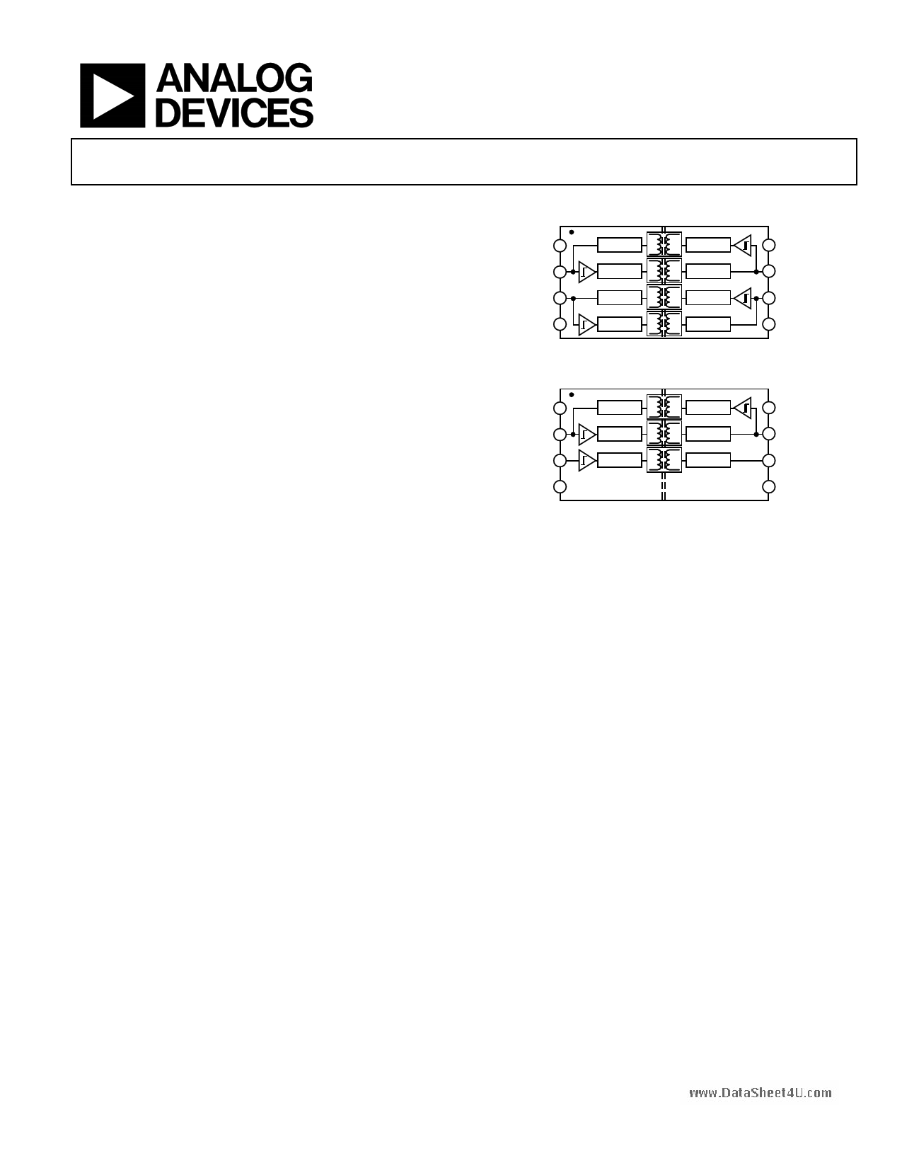
FUNCTIONAL BLOCK DIAGRAMS
VDD1 1
SDA1 2
SCL1 3
GND1 4
DECODE
ENCODE
DECODE
ENCODE
ENCODE
DECODE
ENCODE
DECODE
8 VDD2
7 SDA2
6 SCL2
5 GND2
Figure 1. ADuM1250 Functional Block Diagram
VDD1 1
SDA1 2
SCL1 3
GND1 4
DECODE
ENCODE
ENCODE
ENCODE
DECODE
DECODE
8 VDD2
7 SDA2
6 SCL2
5 GND2
Figure 2. ADuM1251 Functional Block Diagram
Both the ADuM1250 and ADuM1251 contain hot swap
circuitry to prevent glitching data when an unpowered card is
inserted onto an active bus.
These isolators are based on iCoupler® chip scale transformer
technology from Analog Devices, Inc. iCoupler is a magnetic
isolation technology with functional, performance, size, and
power consumption advantages as compared to optocouplers.
With the ADuM1250/ADuM1251, iCoupler channels can be
integrated with semiconductor circuitry, which enables a
complete isolated I2C interface to be provided in a small
form factor.
1 Protected by U.S. Patents 5,952,849 and 6,873,065. Other patents pending.
Rev. 0
Information furnished by Analog Devices is believed to be accurate and reliable. However, no
responsibility is assumed by Analog Devices for its use, nor for any infringements of patents or other
rights of third parties that may result from its use. Specifications subject to change without notice. No
license is granted by implication or otherwise under any patent or patent rights of Analog Devices.
Trademarksandregisteredtrademarksarethepropertyoftheirrespectiveowners.
One Technology Way, P.O. Box 9106, Norwood, MA 02062-9106, U.S.A.
Tel: 781.329.4700
www.analog.com
Fax: 781.461.3113
©2006 Analog Devices, Inc. All rights reserved.
1 page 
www.DataSheet4U.com
ADuM1250/ADuM1251
PACKAGE CHARACTERISTICS
Table 3.
Parameter
Resistance (Input-Output)1
Capacitance (Input-Output)1
Input Capacitance
IC Junction-to-Case Thermal Resistance, Side 1
IC Junction-to-Case Thermal Resistance, Side 2
Symbol Min Typ Max Unit
RI-O 1012 Ω
CI-O 1.0 pF
CI 4.0 pF
θJCI 46 °C/W
θJCO 41 °C/W
Test Conditions
f = 1 MHz
Thermocouple located at center of package
underside
1 The device is considered a 2-terminal device; Pin 1 through Pin 4 are shorted together, and Pin 5 through Pin 8 are shorted together.
REGULATORY INFORMATION
The ADuM1250/ADuM1251 has been approved by the following organizations:
Table 4.
UL
Recognized under 1577 Component
Recognition Program1
Basic insulation, 2500 V rms isolation rating
File E214100
CSA (Pending)
Approved under CSA Component Acceptance
Notice #5A
Basic insulation per CSA 60950-1-03 and IEC
60950-1, 400 V rms (560 V peak) maximum
working voltage
File 205078
VDE (Pending)
Certified according to DIN EN 60747-5-2
(VDE 0884 Part 2):2003-012
Basic insulation,400 V rms (560 V peak)
maximum working voltage
File 2471900-4880-0001
1 In accordance with UL1577, each device is proof tested by applying an insulation test voltage ≥ 3000 V rms for 1 second
(current leakage detection limit = 5 μA).
2 In accordance with DIN EN 60747-5-2, each device is proof tested by applying an insulation test voltage ≥ 1050 V peak for 1 second
(partial discharge detection limit = 5 pC).
INSULATION AND SAFETY-RELATED SPECIFICATIONS
Table 5.
Parameter
Rated Dielectric Insulation Voltage
Minimum External Air Gap (Clearance)
Minimum External Tracking (Creepage)
Minimum Internal Gap (Internal Clearance)
Tracking Resistance (Comparative Tracking Index)
Isolation Group
Symbol Value
2500
L(I01) 4.90 min
L(I02) 4.01 min
0.017 min
CTI >175
IIIa
Unit
V rms
mm
mm
mm
V
Conditions
1 minute duration
Measured from input terminals to output terminals,
shortest distance through air
Measured from input terminals to output terminals,
shortest distance path along body
Insulation distance through insulation
DIN IEC 112/VDE 0303 Part 1
Material Group (DIN VDE 0110, 1/89, Table 1)
Rev. 0 | Page 5 of 12
5 Page 
www.DataSheet4U.com
TYPICAL APPLICATION DIAGRAM
VDD
SDA1
SCL1
GND1
1 ADuM1250 8
27
36
45
V2
SDA2
SCL2
GND2
I2C BUS
Figure 9. Typical Isolated I2C Interface using ADuM1250
MAGNETIC FIELD IMMUNITY
The ADuM1250 is extremely immune to external magnetic
fields. The limitation on the ADuM1250’s magnetic field
immunity is set by the condition in which induced voltage in
the transformer’s receiving coil is sufficiently large to either
falsely set or reset the decoder. The following analysis defines
the conditions under which this may occur. The 3 V operating
condition of the ADuM1250 is examined because it represents
the most susceptible mode of operation.
The pulses at the transformer output have an amplitude greater
than 1.0 V. The decoder has a sensing threshold at about 0.5 V, thus
establishing a 0.5 V margin in which induced voltages can be
tolerated. The voltage induced across the receiving coil is given by
V = (−dβ / dt)∑ Πrn2 ; n = 1, 2, ...N
where:
β is the magnetic flux density (gauss).
N is the number of turns in the receiving coil.
rn is the radius of the nth turn in the receiving coil (cm).
Given the geometry of the receiving coil in the ADuM1250 and
an imposed requirement that the induced voltage is at most
50% of the 0.5 V margin at the decoder, a maximum allowable
magnetic field is calculated, as shown in Figure 10.
100
10
1
0.1
0.01
0.001
1k
10k 100k 1M 10M 100M
MAGNETIC FIELD FREQUENCY (Hz)
Figure 10. Maximum Allowable External Magnetic Flux Density
ADuM1250/ADuM1251
For example, at a magnetic field frequency of 1 MHz, the
maximum allowable magnetic field of 0.2 kgauss induces a
voltage of 0.25 V at the receiving coil. This is about 50% of the
sensing threshold and does not cause a faulty output transition.
Similarly, if such an event occurs during a transmitted pulse
(with the worst-case polarity), it reduces the received pulse
from > 1.0 V to 0.75 V. Note that this is still well above the 0.5 V
sensing threshold of the decoder.
The preceding magnetic flux density values correspond to
specific current magnitudes at given distances away from the
ADuM1250 transformers. Figure 11 expresses these allowable
current magnitudes as a function of frequency for selected
distances. As shown in Figure 11, the ADuM1250 is extremely
immune and can be affected only by extremely large currents
operated at high frequency and very close to the component.
For the 1 MHz example, one would have to place a 0.5 kA
current 5 mm away from the ADuM1250 to affect the
component’s operation.
1000
DISTANCE = 1m
100
10
DISTANCE = 100mm
1
DISTANCE = 5mm
0.1
0.01
1k
10k 100k 1M 10M 100M
MAGNETIC FIELD FREQUENCY (Hz)
Figure 11. Maximum Allowable Current for Various
Current-to-ADuM1250 Spacings
Note that at combinations of strong magnetic fields and high
frequencies, any loops formed by printed circuit board traces
could induce sufficiently large error voltages to trigger the
threshold of succeeding circuitry. Care should be taken in the
layout of such traces to avoid this possibility.
Rev. 0 | Page 11 of 12
11 Page | ||
| Páginas | Total 12 Páginas | |
| PDF Descargar | [ Datasheet ADUM1251.PDF ] | |
Hoja de datos destacado
| Número de pieza | Descripción | Fabricantes |
| ADUM1250 | (ADUM1250 / ADUM1251) Hot Swappable Dual I2C Isolators | Analog Devices |
| ADUM1251 | (ADUM1250 / ADUM1251) Hot Swappable Dual I2C Isolators | Analog Devices |
| Número de pieza | Descripción | Fabricantes |
| SLA6805M | High Voltage 3 phase Motor Driver IC. |
Sanken |
| SDC1742 | 12- and 14-Bit Hybrid Synchro / Resolver-to-Digital Converters. |
Analog Devices |
|
DataSheet.es es una pagina web que funciona como un repositorio de manuales o hoja de datos de muchos de los productos más populares, |
| DataSheet.es | 2020 | Privacy Policy | Contacto | Buscar |