|
|
|
PDF AD8677 Data sheet ( Hoja de datos )
| Número de pieza | AD8677 | |
| Descripción | Maximum Offset Voltage Op Amp | |
| Fabricantes | Analog Devices | |
| Logotipo | ||
Hay una vista previa y un enlace de descarga de AD8677 (archivo pdf) en la parte inferior de esta página. Total 17 Páginas | ||
|
No Preview Available !
130 μV Maximum Offset Voltage
Op Amp in TSOT
AD8677
FEATURES
Low offset voltage: 130 μV max
Input offset drift: 1.5 μV/°C max
Low noise: 0.25 μV p-p
High gain, CMRR and PSRR: 115 dB min
Low supply current: 1.1 mA
Wide supply voltage range: ±4 V to ±18 V operation
APPLICATIONS
Medical and industrial instrumentation
Sensors and controls
Thermocouple
RTDs
Strain bridges
Shunt current measurements
Precision filters
GENERAL DESCRIPTION
The AD8677 is the next generation of precision, ultralow offset
amplifiers. It builds on the high performance of the OP07 and
integrates lower power (1.1 mA typical), lower input bias
current (±1 nA maximum), and higher CMRR/PSRR (130 dB)
in the small TSOT package. Operation is fully specified from ±5
V to ±15 V supply.
The AD8677 provides higher accuracy than industry-standard
OP07-type amplifiers due to Analog Devices’ iPolar™ process,
which supports enhanced performance in a smaller footprint.
These performance enhancements include wider output swing,
lower power, and higher CMRR (common-mode rejection
ratio) and PSRR (power supply rejection ratio). The AD8677
maintains stability of offsets and gain virtually regardless of
variations in time or temperature. Excellent linearity and gain
accuracy can be maintained at high closed-loop gains.
The AD8677 is fully specified over the extended industrial tem-
perature range of −40°C to +125°C. The AD8677 amplifier is
available in the tiny, 5-lead TSOT and the popular 8-lead,
narrow SOIC lead-free packages.
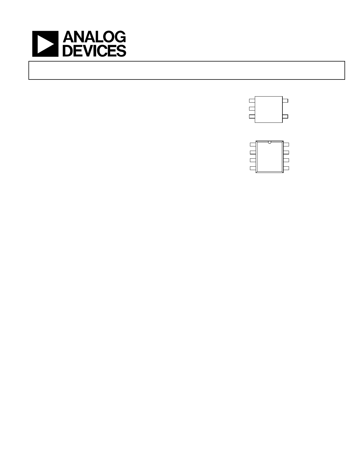
PIN CONFIGURATIONS
OUT 1
V– 2
+IN 3
AD8677
TOP VIEW
(Not to Scale)
5 V+
4 –IN
Figure 1. 5-Lead TSOT (UJ-5)
NULL 1
8 NULL
–IN 2
+IN 3
V– 4
AD8677
TOP VIEW
(Not to Scale)
7 V+
6 OUT
5 NC
NC = NO CONNECT
Figure 2. 8-Lead SOIC_N (R-8)
Rev. A
Information furnished by Analog Devices is believed to be accurate and reliable. However, no
responsibility is assumed by Analog Devices for its use, nor for any infringements of patents or other
rights of third parties that may result from its use. Specifications subject to change without notice. No
license is granted by implication or otherwise under any patent or patent rights of Analog Devices.
Trademarksandregisteredtrademarksarethepropertyoftheirrespectiveowners.
One Technology Way, P.O. Box 9106, Norwood, MA 02062-9106, U.S.A.
Tel: 781.329.4700
www.analog.com
Fax: 781.461.3113 © 2005-2011 Analog Devices, Inc. All rights reserved.
1 page 
AD8677
VS = ±15 V, TA = +25°C, unless otherwise specified.
Table 2.
Parameter
INPUT CHARACTERISTICS
Offset Voltage
Symbol
VOS
Input Bias Current
IB
Input Offset Current
IOS
Input Voltage Range
Common-Mode Rejection Ratio
CMRR
Open Loop Gain
AVO
Offset Voltage Drift
OUTPUT CHARACTERISTICS
Output Voltage Swing
ΔVOS/ΔT
VOUT
Short Circuit Limit
Output Current
POWER SUPPLY
Power Supply Rejection Ratio
Supply Current/Amplifier
DYNAMIC PERFORMANCE
Slew Rate
Gain Bandwidth Product
Phase Margin
NOISE PERFORMANCE
Voltage Noise
Voltage Noise Density
Current Noise Density
ISC
IO
PSRR
ISY
SR
GBP
en p-p
en
in
Test Conditions/Comments
−40°C ≤ TA ≤ +125°C
−40°C ≤ TA ≤ +125°C
−40°C ≤ TA ≤ +125°C
VCM = ±13.0 V
−40°C ≤ TA ≤ +125°C
RL = 2 kΩ to ground, VO = ±11 V
−40°C ≤ TA ≤ +125°C
−40°C ≤ TA ≤ +125°C
RL = 10 kΩ to ground
−40°C ≤ TA ≤ +125°C
RL = 2 kΩ to ground
−40°C ≤ TA ≤ +125°C
VO = 13.5 V
VS = ±4.0 V to ±18.0 V
−40°C ≤ TA ≤ +125°C
VO = 0 V
−40°C ≤ TA ≤ +125°C
RL = 10 kΩ
0.1 Hz to 10 Hz
f = 1 kHz
f = 1 kHz
Min Typ Max Unit
−13.5
120
120
1000
1000
45
0.2
0.2
140
10000
0.5
130
350
1
1
1
1
+13.5
1.5
μV
μV
nA
nA
nA
nA
V
dB
dB
V/mV
V/mV
μV/°C
±13.95
±13.9
±13.75
±13.7
14
13.8
30
15
V
V
V
V
mA
mA
115 130
dB
110 dB
1.1 1.3 mA
1.8 mA
0.2 V/μs
0.6 MHz
80 Degrees
0.25
10
0.074
μV p-p
nV/√Hz
pA/√Hz
Rev. A | Page 4 of 16
5 Page 
AD8677
30
VS = ±5V
VIN = ±50mV
G = +1
25
20
–OS
+OS
15
10
5
0
0 2 4 6 8 10
CLOAD (nF)
Figure 27. Overshoot vs. Capacitive Load
112
VS = ±15V
110
108
106
104
102
100
98
96
100
1k 10k 100k
FREQUENCY (Hz)
Figure 28. CMRR vs. Frequency
100
–PSRR
80
12
1M
60
40
+PSRR
20
0
10
100
1k
10k 100k
1M
FREQUENCY (Hz)
Figure 29. PSRR vs. Frequency
100
VS = ±15V
RVILN==∞28mV
CL = 20pF
10
G = +100
G = +10
1
G = +1
0.1
0.01
10
100 1k 10k 100k
FREQUENCY (Hz)
Figure 30. Output Impedance vs. Frequency
100 VS = ±5V
RVILN==∞28mV
CL = 20pF
10
G = +100
1M
G = +10
1
G = +1
0.1
0.01
10
100 1k 10k 100k
FREQUENCY (Hz)
Figure 31. Output Impedance vs. Frequency
100
VS = ±15V
1M
10
1
0.1 1 10 100
FREQUENCY (Hz)
Figure 32. Voltage Noise Density vs. Frequency
1k
Rev. A | Page 10 of 16
11 Page | ||
| Páginas | Total 17 Páginas | |
| PDF Descargar | [ Datasheet AD8677.PDF ] | |
Hoja de datos destacado
| Número de pieza | Descripción | Fabricantes |
| AD8671 | Low Input Bias Current Operational Amplifiers | Analog Devices |
| AD8672 | Low Input Bias Current Operational Amplifiers | Analog Devices |
| AD8674 | Low Input Bias Current Operational Amplifiers | Analog Devices |
| AD8675 | Rail-to-Rail Output Op Amp | Analog Devices |
| Número de pieza | Descripción | Fabricantes |
| SLA6805M | High Voltage 3 phase Motor Driver IC. |
Sanken |
| SDC1742 | 12- and 14-Bit Hybrid Synchro / Resolver-to-Digital Converters. |
Analog Devices |
|
DataSheet.es es una pagina web que funciona como un repositorio de manuales o hoja de datos de muchos de los productos más populares, |
| DataSheet.es | 2020 | Privacy Policy | Contacto | Buscar |