|
|
|
PDF ADL5322 Data sheet ( Hoja de datos )
| Número de pieza | ADL5322 | |
| Descripción | GaAs Matched RF PA Predriver | |
| Fabricantes | Analog Devices | |
| Logotipo | ||
Hay una vista previa y un enlace de descarga de ADL5322 (archivo pdf) en la parte inferior de esta página. Total 12 Páginas | ||
|
No Preview Available !
www.DataSheet4U.com
FEATURES
Internally matched to 50 Ω input and output
Internally biased
Operating frequency: 700 MHz to 1000 MHz
Gain: 20 dB
OIP3: 45 dBm
P1 dB: 27 dBm
Noise figure: 5 dB
3 mm × 3 mm LFCSP
Power supply: 5 V
APPLICATIONS
CDMA2000, WCDMA, and GSM base station transceivers and
high power amplifiers
GENERAL DESCRIPTION
The ADL5322 is a high linearity GaAs driver amplifier that is
internally matched to 50 Ω for operation in the 700 MHz to
1000 MHz frequency range. The amplifier, which has a gain of
20 dB, is specially designed for use in the output stage of a
cellular base station radio or as an input preamplifier in a
multicarrier base station power amplifier. Matching and biasing
are all on-chip. The ADL5322 is available in a Pb-free, 3mm ×
3 mm, 8-lead LFCSP package with an operating temperature
from −40°C to +85°C.
700 MHz to 1000 MHz GaAs
Matched RF PA Predriver
ADL5322
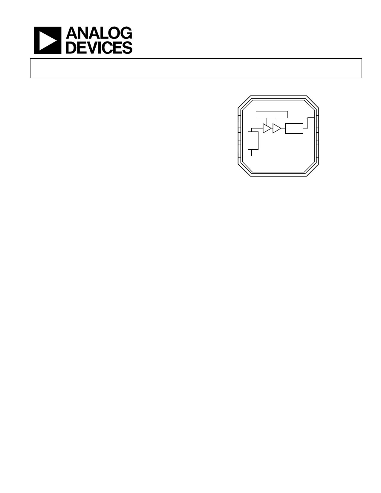
FUNCTIONAL BLOCK DIAGRAM
VCC 5
GND 6
GND 7
RFIN 8
BIAS CONTROL
OUTPUT
MATCH
ADL5322
Figure 1.
4 RFOUT
3 GND
2 VCC
1 VCC
Rev. 0
Information furnished by Analog Devices is believed to be accurate and reliable. However, no
responsibility is assumed by Analog Devices for its use, nor for any infringements of patents or other
rights of third parties that may result from its use. Specifications subject to change without notice. No
license is granted by implication or otherwise under any patent or patent rights of Analog Devices.
Trademarksandregisteredtrademarksarethepropertyoftheirrespectiveowners.
One Technology Way, P.O. Box 9106, Norwood, MA 02062-9106, U.S.A.
Tel: 781.329.4700
www.analog.com
Fax: 781.461.3113
©2006 Analog Devices, Inc. All rights reserved.
1 page 
PIN CONFIGURATION AND FUNCTION DESCRIPTIONS
VCC 1
VCC 2
GND 3
RFOUT 4
PIN 1
INDICATOR
ADL5322
TOP VIEW
(Not to Scale)
8 RFIN
7 GND
6 GND
5 VCC
Figure 2. Pin Configuration
ADL5322
Table 3. Pin Function Descriptions
Pin No. Mnemonic
Description
1, 2, 5 VCC
Positive 5 V Supply Voltage. Bypass these three pins with independent power supply decoupling
networks (100 pF, 10 nF, and 10 μF).
3, 6, 7 GND
Device Ground.
4 RFOUT
RF Output. Internally matched to 50 Ω.
8 RFIN
RF Input. Internally matched to 50 Ω.
N/A EP
Exposed Paddle. Connect to ground plane via a low impedance path.
Table 4. S-Parameters
Frequency
ADL5322 (1, 1)
700.0 MHz
0.210/109.457
720.0 MHz
0.195/104.437
740.0 MHz
0.179/99.101
760.0 MHz
0.165/93.363
780.0 MHz
0.151/86.953
800.0 MHz
0.138/79.928
820.0 MHz
0.125/71.950
840.0 MHz
0.114/62.829
860.0 MHz
0.103/52.162
880.0 MHz
0.095/39.531
900.0 MHz
0.090/24.952
920.0 MHz
0.088/9.188
940.0 MHz
+0.090/−7.350
960.0 MHz
+0.095/−23.642
980.0 MHz
+0.104/−39.131
1.000 GHz
+0.115/−53.477
ADL5322 (1, 2)
0.002/97.018
0.002/93.284
0.002/87.856
0.002/86.137
0.002/78.668
0.002/74.072
0.002/68.940
0.002/62.269
0.002/56.742
0.002/56.696
0.003/43.549
0.003/37.254
0.003/29.904
0.003/24.334
0.003/16.521
0.003/8.139
ADL5322 (2, 1)
+11.221/−158.622
+11.108/−166.579
+11.013/−174.596
10.931/177.282
10.856/169.006
10.781/160.613
10.698/152.065
10.605/143.342
10.493/134.489
10.361/125.433
10.210/116.239
10.033/106.889
9.837/97.326
9.614/87.600
9.364/77.609
9.081/67.342
ADL5322 (2, 2)
0.436/150.470
0.392/145.211
0.345/137.443
0.295/133.051
0.242/125.612
0.187/116.434
0.130/102.897
0.079/76.154
0.061/18.090
+0.098/−26.962
+0.153/−46.741
+0.211/−58.300
+0.269/−66.606
+0.324/−73.265
+0.376/−78.914
+0.424/−83.911
Rev. 0 | Page 5 of 12
5 Page 
OUTLINE DIMENSIONS
3.00
BSC SQ
PIN 1
INDICATOR
TOP
VIEW
0.60 MAX
2.75
BSC SQ
0.50
BSC
8
5
0.50
0.40
0.30 PIN 1
INDICATOR
1
1.50
REF
4
1.89
1.74
1.59
0.90 MAX 12° MAX
0.85 NOM
0.70 MAX
0.65 TYP
0.05 MAX
0.01 NOM
1.60
1.45
1.30
SEATING
PLANE
0.30
0.23
0.18
0.20 REF
Figure 18. 8-Lead Lead Frame Chip Scale Package [LFCSP_VD]
3 mm × 3 mm Body, Very Thin, Dual Lead
(CP-8-2)
Dimensions shown in millimeters
ADL5322
ORDERING GUIDE
Model
Temperature Range
ADL5322ACPZ-R71 −40°C to +85°C
ADL5322ACPZ-WP1 −40°C to +85°C
ADL5322-EVAL
Package Description
8-Lead LFCSP_VD, 7" Tape and Reel
8-Lead LFCSP_VD, Waffle Pack
Evaluation Board
Package Option
CP-8-2
CP-8-2
Branding
OP
OP
Ordering Quantity
1500
50
1
1 Z = Pb-free part.
Rev. 0 | Page 11 of 12
11 Page | ||
| Páginas | Total 12 Páginas | |
| PDF Descargar | [ Datasheet ADL5322.PDF ] | |
Hoja de datos destacado
| Número de pieza | Descripción | Fabricantes |
| ADL5320 | 400 MHz to 2700 MHz RF Driver Amplifier | Analog Devices |
| ADL5321 | 2.3 GHz to 4.0 GHz RF Driver Amplifier | Analog Devices |
| ADL5322 | GaAs Matched RF PA Predriver | Analog Devices |
| ADL5323 | GaAs Matched RF PA Predriver | Analog Devices |
| Número de pieza | Descripción | Fabricantes |
| SLA6805M | High Voltage 3 phase Motor Driver IC. |
Sanken |
| SDC1742 | 12- and 14-Bit Hybrid Synchro / Resolver-to-Digital Converters. |
Analog Devices |
|
DataSheet.es es una pagina web que funciona como un repositorio de manuales o hoja de datos de muchos de los productos más populares, |
| DataSheet.es | 2020 | Privacy Policy | Contacto | Buscar |