|
|
|
PDF IDT71P74204 Data sheet ( Hoja de datos )
| Número de pieza | IDT71P74204 | |
| Descripción | (IDT71P74x04) 18Mb Pipelined QDR II SRAM Burst of 4 | |
| Fabricantes | IDT | |
| Logotipo | ||
Hay una vista previa y un enlace de descarga de IDT71P74204 (archivo pdf) en la parte inferior de esta página. Total 22 Páginas | ||
|
No Preview Available !
www.DataSheet4U.com
Advance
18Mb Pipelined
QDR™II SRAM
Burst of 4
Information
IDT71P74204
IDT71P74104
IDT71P74804
Features
Description
IDT71P74604
x 18Mb Density (2Mx8, 2Mx9, 1Mx18, 512kx36)
The IDT QDRIITM Burst of four SRAMs are high-speed synchronous
x Separate, Independent Read and Write Data Ports
memories with independent, double-data-rate (DDR), read and write
- Supports concurrent transactions
data ports. This scheme allows simultaneous read and write access for
x Dual Echo Clock Output
the maximum device throughput, with four data items passed with each
x 4-Word Burst on all SRAM accesses
read or write. Four data word transfers occur per clock cycle, providing
x Multiplexed Address Bus One Read or One Write request quad-data-rate (QDR) performance. Comparing this with standard SRAM
per clock cycle
common I/O (CIO), single data rate (SDR) devices, a four to one in-
x DDR (Double Data Rate) Data Bus
crease in data access is achieved at equivalent clock speeds. Consider-
- Four word burst data per two clock cycles on
ing that QDRII allows clock speeds in excess of standard SRAM de-
each port
vices, the throughput can be increased well beyond four to one in most
- Four word transfers per clock cycle
applications.
x Depth expansion through Control Logic
Using independent ports for read and write data access, simplifies
x HSTL (1.5V) inputs that can be scaled to receive signals system design by eliminating the need for bi-directional buses. All buses
from 1.4V to 1.9V.
associated with the QDRII are unidirectional and can be optimized for
x Scalable output drivers
signal integrity at very high bus speeds. The QDRII has scalable output
- Can drive HSTL, 1.8V TTL or any voltage level impedance on its data output bus and echo clocks, allowing the user to
from 1.4V to 1.9V.
tune the bus for low noise and high performance.
- Output Impedance adjustable from 35 ohms to 70
The QDRII has a single SDR address bus with read addresses and
ohms write addresses multiplexed. The read and write addresses interleave
x 1.8V Core Voltage (VDD)
with each occurring a maximum of every other cycle. In the event that no
x 165-ball, 1.0mm pitch, 15mm x 17mm fBGA Package
operation takes place on a cycle, the subsequest cycle may begin with
x JTAG Interface
either a read or write. During write operations, the writing of individual
bytes may be blocked through the use of byte or nibble write control
signals.
The QDRII has echo clocks, which provide the user with a clock
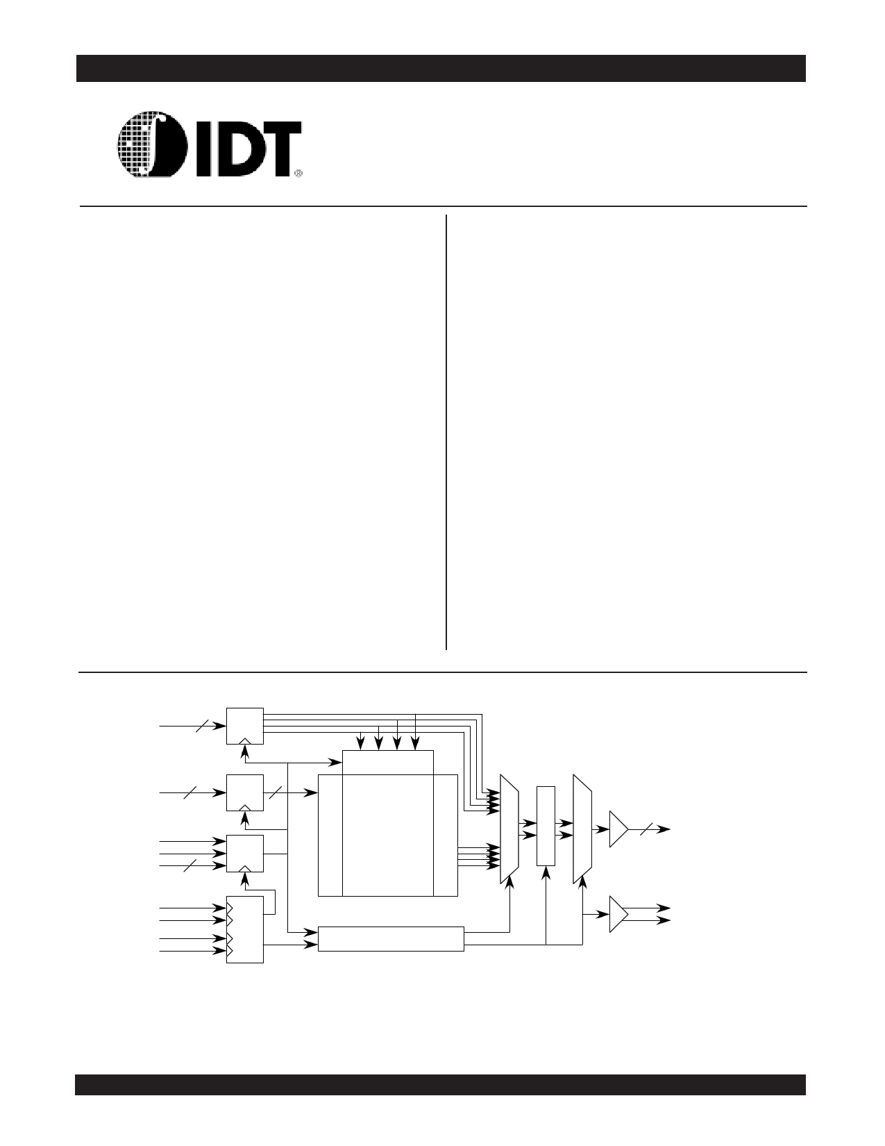
Functional Block Diagram
D
(Note1)
DATA
REG
(Note2)
SA
ADD (Note2)
REG
R CTRL
W (Note3) LOGIC
BWx
WRITE DRIVER
18M
MEMORY
ARRAY
(Note1)
Q
K CLK
K GEN
C SELECT OUTPUT CONTROL
C
CQ
CQ
6111 drw16
Notes
1) Represents 8 data signal lines for x8, 9 signal lines for x9, 18 signal lines for x18, and 36 signal lines for x36
2) Represents 19 address signal lines for x8 and x9, 18 address signal lines for x18, and 17 address signal lines for x36.
3) Represents 1 signal line for x9, 2 signal lines for x18, and four signal lines for x36. On x8 parts, the BW is a “nibble write”
and there are 2 signal lines.
MARCH
2004
1
©2003 Integrated Device Technology, Inc. “QDR SRAMs and Quad Data Rate RAMs comprise a new family of products developed by Cypress Semiconductor, IDT, and Micron Technology, Inc. “ DSC-6111/00
1 page 
IDT71P74204 (2M x 8-Bit), 71P74104 (2M x 9-Bit), 71P74804 (1M x 18-Bit) 71P74604 (512K x 36-Bit)
Advance Information
18 Mb QDR II SRAM Burst of 4
Commercial Temperature Range
Pin Configuration 2M x 8
1 2 3 4 5 6 7 8 9 10 11
A
CQ VSS/
SA
W NW1 K
NC
R
SA VSS/ CQ
SA (2)
SA (1)
B NC NC NC SA NC K NW0 SA NC NC Q3
C NC NC NC VSS SA NC SA VSS NC NC D3
D NC D4 NC VSS VSS VSS VSS VSS NC NC NC
E
NC NC
Q4
VDDQ
VSS
VSS
VSS VDDQ
NC
D2
Q2
F NC NC NC VDDQ VDD VSS VDD VDDQ NC NC NC
G
NC
D5
Q5
VDDQ
VDD
VSS
VDD VDDQ
NC
NC NC
H
Doff
VREF
VDDQ
VDDQ
VDD
VSS
VDD
VDDQ
VDDQ
VREF
ZQ
J NC NC NC VDDQ VDD VSS VDD VDDQ NC Q1 D1
K NC NC NC VDDQ VDD VSS VDD VDDQ NC NC NC
L
NC Q6
D6
VDDQ
VSS
VSS
VSS VDDQ
NC
NC
Q0
M NC NC NC VSS VSS VSS VSS VSS NC NC D0
N NC D7 NC VSS SA SA SA VSS NC NC NC
P NC NC Q7 SA SA C SA SA NC NC NC
R TDO TCK SA SA SA C SA SA SA TMS TDI
6111 tbl 12
165-ball FBGA Pinout
TOP VIEW
NOTES:
1. A10 is reserved for the 36Mb expansion address.
2. A2 is reserved for the 72Mb expansion address.
6.542
5 Page 
IDT71P74204 (2M x 8-Bit), 71P74104 (2M x 9-Bit), 71P74804 (1M x 18-Bit) 71P74604 (512K x 36-Bit)
Advance Information
18 Mb QDR II SRAM Burst of 4
Commercial Temperature Range
DC Electrical Characteristics Over the Operating Temperature and
Supply Voltage Range (VDD = 1.8 ± 100mV, VDDQ = 1.4V to 1.9V)
P aram eter
S ym bol
Test Conditions
Min Max Unit Note
Inp ut Le akag e Curre nt
IIL V DD = M ax V IN = VSS to VDD Q
-10 +10 µA
Outp ut Le akag e Curre nt
IOL Outp ut Disab le d
-10 +10 µA
Op e rating Curre nt
(x36,x18,x9,x8): DDR
Stand b y Curre nt: NOP
Output High Voltage
333M HZ
-
VDD = Max,
IDD IO UT = 0m A (o utp uts o p e n),
Cyc le Tim e > tKHKH M in
300M HZ
250M HZ
300MHz
-
-
-
167MHz
-
333M HZ
-
Device Des ele cted (in NOP state) 300M HZ
IS B1
IO UT = 0m A (outputs o pen),
f=M ax,
250M HZ
All Inputs <0.2V or > V DD -0.2V 200M Hz
-
-
-
167MHz
-
V O H1 RQ = 250Ω, IOH = -15m A
V DD Q / 2-0 .1 2
TB D
TB D
TB D
TB D
TB D
TB D
TB D
TB D
TB D
TB D
V DD Q /2+ 0.12
mA
mA
V
1
2
3,7
Output Low Voltage
V OL1 RQ = 250Ω, IOL = 15mA
V DD Q / 2-0 .1 2
V DD Q /2+ 0.12
V
4,7
Output High Voltage
VO H2 IOH = -0.1m A
V DD Q -0.2
V DD Q
V
5
Output Low Voltage
VOL2 IOL = 0.1m A
VSS 0.2 V 6
NOTES:
1. Operating Current is measured at 100% bus utilization.
2. Standby Current is only after all pending read and write burst operations are completed.
3. Outputs are impedance-controlled. IOH = -(VDDQ/2)/(RQ/5) and is guaranteed by device characterization for 175Ω < RQ < 350Ω. This
parameter is tested at RQ = 250Ω, which gives a nominal 50Ω output impedance.
4. Outputs are impedance-controlled. IOL = (VDDQ/2)/(RQ/5) and is guaranteed by device characterization for 175Ω < RQ < 350Ω. This
parameter is tested at RQ = 250Ω, which gives a nominal 50Ω output impedance.
5. This measurement is taken to ensure that the output has the capability of pulling to the VDDQ rail, and is not intended to be used as an
impedance measurement point.
6. This measurement is taken to ensure that the output has the capability of pulling to Vss, and is not intended to be used as an impedance
measurement point.
7. Programmable Impedance Mode.
6111 tb l 10 c
61.412
11 Page | ||
| Páginas | Total 22 Páginas | |
| PDF Descargar | [ Datasheet IDT71P74204.PDF ] | |
Hoja de datos destacado
| Número de pieza | Descripción | Fabricantes |
| IDT71P74204 | (IDT71P74x04) 18Mb Pipelined QDR II SRAM Burst of 4 | IDT |
| Número de pieza | Descripción | Fabricantes |
| SLA6805M | High Voltage 3 phase Motor Driver IC. |
Sanken |
| SDC1742 | 12- and 14-Bit Hybrid Synchro / Resolver-to-Digital Converters. |
Analog Devices |
|
DataSheet.es es una pagina web que funciona como un repositorio de manuales o hoja de datos de muchos de los productos más populares, |
| DataSheet.es | 2020 | Privacy Policy | Contacto | Buscar |