|
|
|
PDF AD8668 Data sheet ( Hoja de datos )
| Número de pieza | AD8668 | |
| Descripción | 4 MHz RR0 Amplifiers | |
| Fabricantes | Analog Devices | |
| Logotipo | ||
Hay una vista previa y un enlace de descarga de AD8668 (archivo pdf) en la parte inferior de esta página. Total 16 Páginas | ||
|
No Preview Available !
FEATURES
Offset voltage: 2.5 mV max
Low input bias current: 1 pA max
Single-supply operation: 5 V to 16 V
Dual-supply operation: ±2.5 V to ±8 V
Low noise: 8 nV/√Hz @ 10 kHz
Wide bandwidth: 4 MHz
Rail-to-rail output
Unity-gain stable
Lead-free packaging
AD8666/AD8668 qualified for automotive applications
APPLICATIONS
Sensor amplification
Reference buffers
Medical equipment
Physiological measurements
Signal filters and conditioning
Consumer audio
Photodiode amplification
ADC driver
Level shifting circuits
GENERAL DESCRIPTION
The AD866x family is single supply, rail-to-rail output
amplifiers with low noise performance featuring an extended
operating range with supply voltages up to 16 V. They also
feature low input bias currents, wide signal bandwidth, and low
input voltage and current noise. For lower offset voltage, choose
the AD8661/AD8662/AD8664 family.
The combination of low offsets, very low input bias currents,
and wide supply range make these amplifiers useful in a wide
variety of cost sensitive applications normally associated with
much higher priced JFET amplifiers. Systems using high
impedance sensors, such as photo diodes, benefit from the
combination of low input bias current, low noise, and low offset
and bandwidth. The wide operating voltage range matches high
performance ADCs and DACs. Audio applications and medical
monitoring equipment can take advantage of the high input
impedance, low voltage and current noise, wide bandwidth, and
the lack of popcorn noise found in many other low input bias
current amplifiers.
The AD866x family is specified over the extended industrial
temperature range (−40°C to +125°C). See the Ordering Guide
for automotive models.
16 V, 4 MHz RR0 Amplifiers
AD8665/AD8666/AD8668
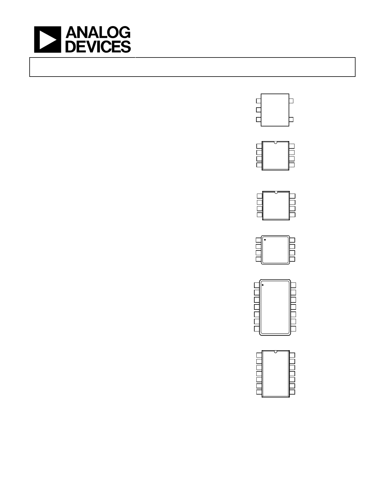
PIN CONFIGURATIONS
OUT 1
5 V+
AD8665
V– 2 TOP VIEW
(Not to Scale)
+IN 3
4 –IN
Figure 1. AD8665, 5-Lead SOT-23 (RJ-5)
NC
–IN
+IN
VEE
1 8 NC
2 AD8665 7 VCC
3 TOP VIEW 6 OUT
4 (Not to Scale) 5 NC
NC = NO CONNECT
Figure 2. AD8665, 8-Lead SOIC_N (R-8)
OUT A
–IN A
+IN A
V–
1
2 AD8666
3 TOP VIEW
4 (Not to Scale)
8 V+
7 OUT B
6 –IN B
5 +IN B
Figure 3. AD8666, 8-Lead SOIC_N (R-8)
OUT A 1
8 V+
–IN A 2 AD8666 7 OUT B
+IN A 3 TOP VIEW 6 –IN B
V– 4 (Not to Scale) 5 +IN B
Figure 4. AD8666, 8-Lead MSOP (RM-8)
OUT A 1
IN A 2
+IN A 3
V+ 4
+IN B 5
–IN B 6
OUT B 7
AD8668
TOP VIEW
(Not to Scale)
14 OUT D
13 –IN D
12 +IN D
11 V–
10 +IN C
9 –IN C
8 OUT C
Figure 5. AD8668, 14-Lead TSSOP (RU-14)
OUT A
–IN A
+IN A
V+
+IN B
–IN B
OUT B
1 14 OUT D
2 13 –IN D
3 AD86468 12 +IN D
4 TOP VIEW 11 V–
5 (Not to Scale) 10 +IN C
6 9 –IN C
7 8 OUT C
Figure 6. AD8668, 14-Lead SOIC_N (R-14)
Rev. B
Information furnished by Analog Devices is believed to be accurate and reliable. However, no
responsibilityisassumedbyAnalogDevices for itsuse,nor foranyinfringementsofpatentsor other
rights of third parties that may result from its use. Specifications subject to change without notice. No
license is granted by implication or otherwise under any patent or patent rights of Analog Devices.
Trademarksandregisteredtrademarksarethepropertyoftheirrespectiveowners.
One Technology Way, P.O. Box 9106, Norwood, MA 02062-9106, U.S.A.
Tel: 781.329.4700
www.analog.com
Fax: 781.461.3113 ©2006–2011 Analog Devices, Inc. All rights reserved.
1 page 
ABSOLUTE MAXIMUM RATINGS
Table 3.
Parameter
Supply Voltage
Input Voltage
Differential Input Voltage
Output Short-Circuit to GND
Storage Temperature Range
Operating Temperature Range
Lead Temperature (Soldering, 60 sec)
Junction Temperature
Rating
18 V
GND to VDD
±18 V
Indefinite
−65°C to +150°C
−40°C to +125°C
300°C
150°C
Stresses above those listed under Absolute Maximum Ratings
may cause permanent damage to the device. This is a stress
rating only; functional operation of the device at these or any
other conditions above those indicated in the operational
section of this specification is not implied. Exposure to absolute
maximum rating conditions for extended periods may affect
device reliability.
AD8665/AD8666/AD8668
THERMAL RESISTANCE
Table 4. Thermal Resistance
Package Type
5-Lead SOT-23 (RJ-5)
8-Lead SOIC_N (R-8)
8-Lead MSOP (RM-8)
14-Lead SOIC (R-14)
14-Lead TSSOP (RU-14)
θJA
240
158
210
120
180
ESD CAUTION
θJC
92
43
45
36
35
Unit
°C/W
°C/W
°C/W
°C/W
°C/W
Rev. B | Page 5 of 16
5 Page 
100mV
0V
0V
VIN
VDD = ±2.5V
AV = –100
–2.5V
VOUT
TIME (4µs/DIV)
Figure 37. Negative Overload Recovery Time
2.0
VOUT = VDD/2
1.8
1.6
1.4
VDD = 16V
1.2
VDD = 5V
1.0
0.8
0.6
0.4
0.2
0
–40 –20
0
20 40 60 80 100
TEMPERATURE (°C)
Figure 38. Supply Current vs. Temperature
120
AD8665/AD8666/AD8668
2.00
1.75
1.50
1.25
1.00
0.75
0.50
0.25
0
0 2 4 6 8 10 12 14
SUPPLY VOLTAGE (V)
Figure 39. Supply Current vs. Supply Voltage
16
10
8 VIN
6 VOUT
VDD = ±8V
AV = +1
4
2
0
–2
–4
–6
–8
–10
TIME (10µs/DIV)
Figure 40. No Output Phase Reversal
Rev. B | Page 11 of 16
11 Page | ||
| Páginas | Total 16 Páginas | |
| PDF Descargar | [ Datasheet AD8668.PDF ] | |
Hoja de datos destacado
| Número de pieza | Descripción | Fabricantes |
| AD8661 | Rail-to-Rail Operational Amplifiers | Analog Devices |
| AD8662 | Rail-to-Rail Operational Amplifiers | Analog Devices |
| AD8663 | (AD8663 - AD8669) Rail-to-Rail Operational Amplifier | Analog Devices |
| AD8664 | Rail-to-Rail Operational Amplifiers | Analog Devices |
| Número de pieza | Descripción | Fabricantes |
| SLA6805M | High Voltage 3 phase Motor Driver IC. |
Sanken |
| SDC1742 | 12- and 14-Bit Hybrid Synchro / Resolver-to-Digital Converters. |
Analog Devices |
|
DataSheet.es es una pagina web que funciona como un repositorio de manuales o hoja de datos de muchos de los productos más populares, |
| DataSheet.es | 2020 | Privacy Policy | Contacto | Buscar |