|
|
|
PDF NB4L6254 Data sheet ( Hoja de datos )
| Número de pieza | NB4L6254 | |
| Descripción | Differential LVPECL 2x2 Clock Switch and Low Skew Fanout Buffer | |
| Fabricantes | ON Semiconductor | |
| Logotipo | ||
Hay una vista previa y un enlace de descarga de NB4L6254 (archivo pdf) en la parte inferior de esta página. Total 11 Páginas | ||
|
No Preview Available !
NB4L6254
2.5V / 3.3V Differential
LVPECL 2x2 Clock Switch
and Low Skew Fanout
Buffer
Description
The NB4L6254 is a differential 2x2 clock switch and drives
precisely aligned clock signals through its LVPECL fanout buffers. It
employs a fully differential architecture with bipolar technology,
offers superior digital signal characteristics, has very low clock output
skew and supports clock frequencies from DC up to 3.0 GHz.
The NB4L6254 is designed for the most demanding, skew critical
differential clock distribution systems. Typical applications for the
NB4L6254 are clock distribution, switching and data loopback
systems of high−performance computer, networking and
telecommunication systems, as well as on−board clocking of OC−3,
OC−12 and OC−48 communication systems. In addition, the
NB4L6254 can be configured as a single 1:6 or dual 1:3 LVPECL
fanout buffer.
The NB4L6254 can be operated from a single 3.3 V or 2.5 V power
supply.
Features
• Maximum Clock Input Frequency, 3 GHz
• Maximum Input Data Rate, 3 Gb/s
• Differential LVPECL Inputs and Outputs
• Low Output Skew: 50 ps Maximum Output−to−Output Skew
• Synchronous Output Enable Eliminating Output Runt Pulse
Generation and Metastability
• Operating Range: Single 3.3 V or 2.5 V Supply
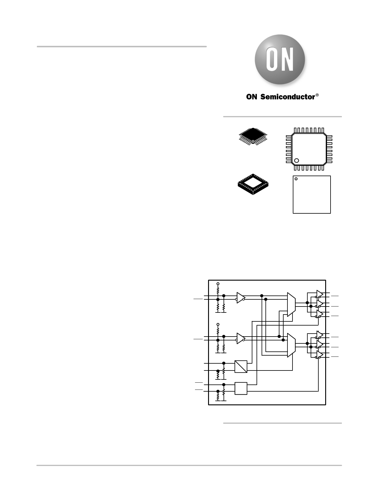
CLK0
CLK0
VCC = 2.375 V to 3.465 V
• LVCMOS Compatible Control Inputs
• Packaged in LQFP−32
• Fully Differential Architecture
• −40°C to 85°C Ambient Operating Temperature
CLK1
CLK1
• These are Pb−Free Devices*
SEL0
SEL1
OEA
OEB
http://onsemi.com
MARKING DIAGRAMS*
LQFP−32
FA SUFFIX
CASE 873A
NB4L
6254
AWLYYWWG
1
1 32
NB4L6254
AWLYYWWG
G
QFN32
MN SUFFIX
CASE 488AM
A = Assembly Location
WL = Wafer Lot
YY = Year
WW = Work Week
G or G = Pb−Free Package
(Note: Microdot may be in either location)
*For additional marking information, refer to
Application Note AND8002/D.
VCC
Bank A
0
1
QA0
QA0
QA1
QA1
QA2
QA2
VCC
Bank B
0
1
QB0
QB0
QB1
QB1
QB2
QB2
SYNC
*For additional information on our Pb−Free strategy and soldering details, please
download the ON Semiconductor Soldering and Mounting Techniques
Reference Manual, SOLDERRM/D.
Figure 1. Functional Block Diagram
ORDERING INFORMATION
See detailed ordering and shipping information in the package
dimensions section on page 9 of this data sheet.
© Semiconductor Components Industries, LLC, 2009
March, 2009 − Rev. 3
1
Publication Order Number:
NB4L6254/D
1 page 
NB4L6254
Table 6. DC CHARACTERISTICS VCC = 2.375 V to 3.465 V, GND = 0 V, TA = −40°C to +85°C
Symbol
Characteristic
Min
Typ
Max Unit
POWER SUPPLY CURRENT
IGND
Power Supply Current (Outputs Open)
LVPECL CLOCK OUTPUTS
60 85 mA
VOH LVPECL Output HIGH Voltage (Notes 4, 5)
VOL LVPECL Output LOW Voltage (Notes 4, 5)
VCC = 3.3 V
VCC = 2.5 V
VCC = 3.3 V
VCC = 2.5 V
VCC − 1145
2155
1355
VCC − 1945
1355
555
VCC − 1020
2280
1480
VCC − 1770
1530
730
VCC – 895
2405
1605
VCC − 1600
1700
900
mV
mV
CLOCK INPUTS
VPP Dynamic Differential Input Voltage (Clock Inputs)
VCMR
Differential Cross−point Voltage (Clock Inputs)
LVCMOS CONTROL INPUTS
0.1 1.3 V
1.0
VCC − 0.3
V
VIH Output HIGH Voltage (LVTTL/LVCMOS)
VIL Output LOW Voltage (LVTTL/LVCMOS)
IIH Input Current VIN = VCC or VIN = GND
2.0
−100
0.8
+100
V
V
mA
NOTE: Device will meet the specifications after thermal equilibrium has been established when mounted in a test socket or printed circuit
board with maintained transverse airflow greater than 500 lfpm. Electrical parameters are guaranteed only over the declared
operating temperature range. Functional operation of the device exceeding these conditions is not implied. Device specification limit
values are applied individually under normal operating conditions and not valid simultaneously.
4. LVPECL Outputs loaded with 50 W termination resistors to VTT = VCC – 2.0 V for proper operation.
5. LVPECL Output parameters vary 1:1 with VCC.
http://onsemi.com
5
5 Page 
NB4L6254
PACKAGE DIMENSIONS
QFN32 5*5*1 0.5 P
CASE 488AM−01
ISSUE O
PIN ONE
LOCATION
ÉÉÉÉD
A
B
E
2 X 0.15 C
2 X 0.15 C
TOP VIEW
0.10 C
(A3)
32 X 0.08 C
SIDE VIEW A1
A
SEATING
PLANE
C
NOTES:
1. DIMENSIONS AND TOLERANCING PER
ASME Y14.5M, 1994.
2. CONTROLLING DIMENSION: MILLIMETERS.
3. DIMENSION b APPLIES TO PLATED
TERMINAL AND IS MEASURED BETWEEN
0.25 AND 0.30 MM TERMINAL
4. COPLANARITY APPLIES TO THE EXPOSED
PAD AS WELL AS THE TERMINALS.
MILLIMETERS
DIM MIN NOM MAX
A 0.800 0.900 1.000
A1 0.000 0.025 0.050
A3 0.200 REF
b 0.180 0.250 0.300
D 5.00 BSC
D2 2.950 3.100 3.250
E 5.00 BSC
E2 2.950 3.100 3.250
e 0.500 BSC
K 0.200 −−− −−−
L 0.300 0.400 0.500
L
32 X
EXPOSED PAD
9
D2
16 17
K
32 X
8
E2
1
32
32 X b
0.10 C A B
0.05 C
24
25
e
SOLDERING FOOTPRINT*
5.30
32 X
0.63
3.20
3.20 5.30
BOTTOM VIEW
32 X
0.28
28 X
0.50 PITCH
*For additional information on our Pb−Free strategy and soldering
details, please download the ON Semiconductor Soldering and
Mounting Techniques Reference Manual, SOLDERRM/D.
ECLinPS is a trademark of Semiconductor Components INdustries, LLC (SCILLC).
ON Semiconductor and
are registered trademarks of Semiconductor Components Industries, LLC (SCILLC). SCILLC reserves the right to make changes without further notice
to any products herein. SCILLC makes no warranty, representation or guarantee regarding the suitability of its products for any particular purpose, nor does SCILLC assume any liability
arising out of the application or use of any product or circuit, and specifically disclaims any and all liability, including without limitation special, consequential or incidental damages.
“Typical” parameters which may be provided in SCILLC data sheets and/or specifications can and do vary in different applications and actual performance may vary over time. All
operating parameters, including “Typicals” must be validated for each customer application by customer’s technical experts. SCILLC does not convey any license under its patent
rights nor the rights of others. SCILLC products are not designed, intended, or authorized for use as components in systems intended for surgical implant into the body, or other
applications intended to support or sustain life, or for any other application in which the failure of the SCILLC product could create a situation where personal injury or death may occur.
Should Buyer purchase or use SCILLC products for any such unintended or unauthorized application, Buyer shall indemnify and hold SCILLC and its officers, employees, subsidiaries,
affiliates, and distributors harmless against all claims, costs, damages, and expenses, and reasonable attorney fees arising out of, directly or indirectly, any claim of personal injury
or death associated with such unintended or unauthorized use, even if such claim alleges that SCILLC was negligent regarding the design or manufacture of the part. SCILLC is an
Equal Opportunity/Affirmative Action Employer. This literature is subject to all applicable copyright laws and is not for resale in any manner.
PUBLICATION ORDERING INFORMATION
LITERATURE FULFILLMENT:
Literature Distribution Center for ON Semiconductor
P.O. Box 5163, Denver, Colorado 80217 USA
Phone: 303−675−2175 or 800−344−3860 Toll Free USA/Canada
Fax: 303−675−2176 or 800−344−3867 Toll Free USA/Canada
Email: [email protected]
N. American Technical Support: 800−282−9855 Toll Free
USA/Canada
Japan: ON Semiconductor, Japan Customer Focus Center
2−9−1 Kamimeguro, Meguro−ku, Tokyo, Japan 153−0051
Phone: 81−3−5773−3850
http://onsemi.com
11
ON Semiconductor Website: http://onsemi.com
Order Literature: http://www.onsemi.com/litorder
For additional information, please contact your
local Sales Representative.
NB4L6254/D
11 Page | ||
| Páginas | Total 11 Páginas | |
| PDF Descargar | [ Datasheet NB4L6254.PDF ] | |
Hoja de datos destacado
| Número de pieza | Descripción | Fabricantes |
| NB4L6254 | Differential LVPECL 2x2 Clock Switch and Low Skew Fanout Buffer | ON Semiconductor |
| Número de pieza | Descripción | Fabricantes |
| SLA6805M | High Voltage 3 phase Motor Driver IC. |
Sanken |
| SDC1742 | 12- and 14-Bit Hybrid Synchro / Resolver-to-Digital Converters. |
Analog Devices |
|
DataSheet.es es una pagina web que funciona como un repositorio de manuales o hoja de datos de muchos de los productos más populares, |
| DataSheet.es | 2020 | Privacy Policy | Contacto | Buscar |