|
|
|
PDF AD8504 Data sheet ( Hoja de datos )
| Número de pieza | AD8504 | |
| Descripción | Micropower CMOS Operational Amplifiers | |
| Fabricantes | Analog Devices | |
| Logotipo | ||
Hay una vista previa y un enlace de descarga de AD8504 (archivo pdf) en la parte inferior de esta página. Total 16 Páginas | ||
|
No Preview Available !
FEATURES
Supply current: 1 μA maximum/amplifier
Offset voltage: 3 mV maximum
Single-supply or dual-supply operation
Rail-to-rail input and output
No phase reversal
Unity gain stable
APPLICATIONS
Portable equipment
Remote sensors
Low power filters
Threshold detectors
Current sensing
GENERAL DESCRIPTION
The AD8502/AD8504 are low power, precision CMOS operational
amplifiers featuring a maximum supply current of 1 μA per
amplifier. The AD8502/AD8504 have a maximum offset voltage
of 3 mV and a typical input bias current of 1 pA operating rail-
to-rail on both the input and output. The AD8502/AD8504 can
operate from a single-supply voltage of +1.8 V to +5.5 V or a
dual-supply voltage of ±0.9 V to ±2.75 V.
With its low power consumption, low input bias current, and
rail-to-rail input and output, the AD8502/AD8504 are ideally
suited for a variety of battery-powered portable applications.
Potential applications include bedside monitors, pulse monitors,
glucose meters, smoke and fire detectors, vibration monitors,
and backup battery sensors.
The ability to swing rail-to-rail at both the input and output
helps maximize dynamic range and signal-to-noise ratio in
systems that operate at very low voltages. The low offset voltage
allows use of the AD8502/AD8504 in systems with high gain
1 μA Micropower CMOS
Operational Amplifiers
AD8502/AD8504
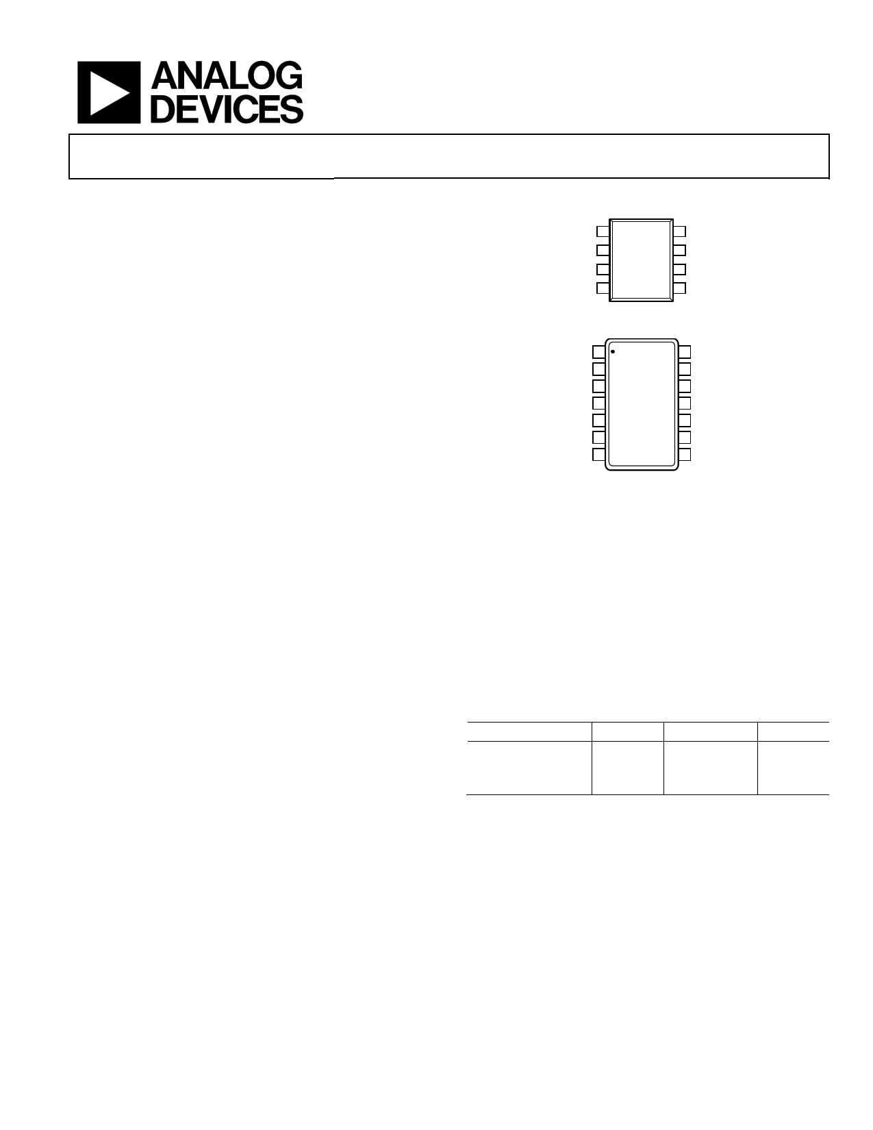
PIN CONFIGURATIONS
OUT A 1
8 V+
–IN A 2 AD8502 7 OUT B
+IN A
3
TOP VIEW
(Not to Scale)
6
–IN B
V– 4
5 +IN B
Figure 1. 8-Lead SOT-23
OUT A 1
–IN A 2
+IN A 3
V+ 4
+IN B 5
–IN B 6
OUT B 7
AD8504
TOP VIEW
(Not to Scale)
14 OUT D
13 –IN D
12 +IN D
11 V–
10 +IN C
9 –IN C
8 OUT C
Figure 2. 14-Lead TSSOP (RU-14)
without creating excessively large output offset errors. The
AD8502 and AD8504 offer an additional benefit by providing
high accuracy without the need for system calibration.
The AD8502/AD8504 are fully specified over the industrial
temperature range (−40°C to +85°C) and the extended indus-
trial temperature range (−40°C to +125°C). The AD8502 is
available in an 8-lead, SOT-23 surface-mount package. The
AD8504 is available in a 14-lead TSSOP surface-mount package.
Table 1. Low Supply Current Op Amps
Supply Current
1 μA
10 μA
Single
AD8500
Dual AD8502 ADA4505-2
Quad
AD8504 ADA4505-4
20 μA
AD8506
AD8508
Rev. A
Information furnished by Analog Devices is believed to be accurate and reliable. However, no
responsibility is assumed by Analog Devices for its use, nor for any infringements of patents or other
rights of third parties that may result from its use. Specifications subject to change without notice. No
license is granted by implication or otherwise under any patent or patent rights of Analog Devices.
Trademarksandregisteredtrademarksarethepropertyoftheirrespectiveowners.
One Technology Way, P.O. Box 9106, Norwood, MA 02062-9106, U.S.A.
Tel: 781.329.4700
www.analog.com
Fax: 781.461.3113 ©2007–2009 Analog Devices, Inc. All rights reserved.
1 page 
Parameter
DYNAMIC PERFORMANCE
Slew Rate
Gain Bandwidth Product
Phase Margin
NOISE PERFORMANCE
Peak-to-Peak Noise
Voltage Noise Density
Current Noise Density
Symbol Conditions
SR RLOAD = 1 MΩ
GBP
ØO
0.1 Hz to 10 Hz
en f = 1 kHz
in f = 1 kHz
AD8502/AD8504
Min Typ Max Unit
0.004
7
60
V/μs
kHz
Degrees
6 μV p-p
190 nV/√Hz
0.1 pA/√Hz
Rev. A | Page 5 of 16
5 Page 
1000
800
600
400
200
0
–200
–400
–600
–800
–1000
0
0.3 0.6 0.9 1.2 1.5 1.8
VCM (V)
Figure 27. Input Offset Voltage vs. Input Common-Mode Voltage, VS = 1.8 V
1000
100
IB (+125°C)
10
IB (+85°C)
1
IB (+25°C)
0.1
0.01
0.001
0
IB (–40°C)
0.3 0.6 0.9 1.2 1.5 1.8
VCM (V)
Figure 28. Input Bias Current vs. Input Common-Mode Voltage, VS = 1.8 V
70
60
50
40
30
20
10
0
0.4 0.5 0.6 0.7 0.8
ISY (µA)
Figure 29. Supply Current Distribution, VS = 1.8 V
0.9
AD8502/AD8504
700
650
600
550
500
0
0.3 0.6 0.9 1.2 1.5 1.8
VCM (V)
Figure 30. Supply Current vs. Input Common-Mode Voltage, VS = 1.8 V
1000
100
SOURCE
10
SINK
1
0.1
0.01
0.001
0.01 0.1
LOAD CURRENT (mA)
1
Figure 31. Output Saturation Voltage vs. Load Current VS = 1.8 V
100
VOH @ 10kΩ LOAD
10
VOL @ 10kΩ LOAD
VOH @ 100kΩ LOAD
1 VOL @ 100kΩ LOAD
0.1
–40
–15 10
35
TEMPERATURE (°C)
60
85
Figure 32. Output Saturation Voltage vs. Temperature, VS = 1.8 V
Rev. A | Page 11 of 16
11 Page | ||
| Páginas | Total 16 Páginas | |
| PDF Descargar | [ Datasheet AD8504.PDF ] | |
Hoja de datos destacado
| Número de pieza | Descripción | Fabricantes |
| AD8500 | Micropower Precision CMOS Operational Amplifier | Analog Devices |
| AD8502 | Micropower CMOS Operational Amplifiers | Analog Devices |
| AD8504 | Micropower CMOS Operational Amplifiers | Analog Devices |
| AD8505 | Zero Input Crossover Distortion Amplifiers | Analog Devices |
| Número de pieza | Descripción | Fabricantes |
| SLA6805M | High Voltage 3 phase Motor Driver IC. |
Sanken |
| SDC1742 | 12- and 14-Bit Hybrid Synchro / Resolver-to-Digital Converters. |
Analog Devices |
|
DataSheet.es es una pagina web que funciona como un repositorio de manuales o hoja de datos de muchos de los productos más populares, |
| DataSheet.es | 2020 | Privacy Policy | Contacto | Buscar |