|
|
|
PDF ADS1225 Data sheet ( Hoja de datos )
| Número de pieza | ADS1225 | |
| Descripción | (ADS1225 / ADS1226) 24-Bit Analog-to-Digital Converter | |
| Fabricantes | Burr-Brown | |
| Logotipo | ||
Hay una vista previa y un enlace de descarga de ADS1225 (archivo pdf) en la parte inferior de esta página. Total 24 Páginas | ||
|
No Preview Available !
www.DataSheet4U.com
BurrĆBrown Products
from Texas Instruments
ADS1225 ¨
ADS1226 ¨
ADS1225
ADS1226
SBAS346 – MAY 2006
24-Bit Analog-to-Digital Converter
with One- and Two-Channel Differential Inputs and Internal Oscillator
FEATURES
• 100SPS Data Rate (High-Speed Mode)
• Single-Cycle Settling
• Easy Conversion Control with START Pin
• Automatic Shutdown
• Low Noise: 4µVRMS Noise (High-Resolution
Mode)
• Input Multiplexer with Two Differential
Channels (ADS1226)
• Voltage Reference Supports Ratiometric
Measurements
• Self-Calibrating
• Simple Read-Only 2-Wire Serial Interface
• Internal High-Impedance Input Buffer
• Internal Temperature Sensor
• Internal Oscillator
• Low-Power: 1mW While Operating, < 1µA
During Shutdown
• Analog and Digital Supplies: 2.7V to 5.5V
APPLICATIONS
• Hand-Held Instrumentation
• Portable Medical Equipment
• Industrial Process Control
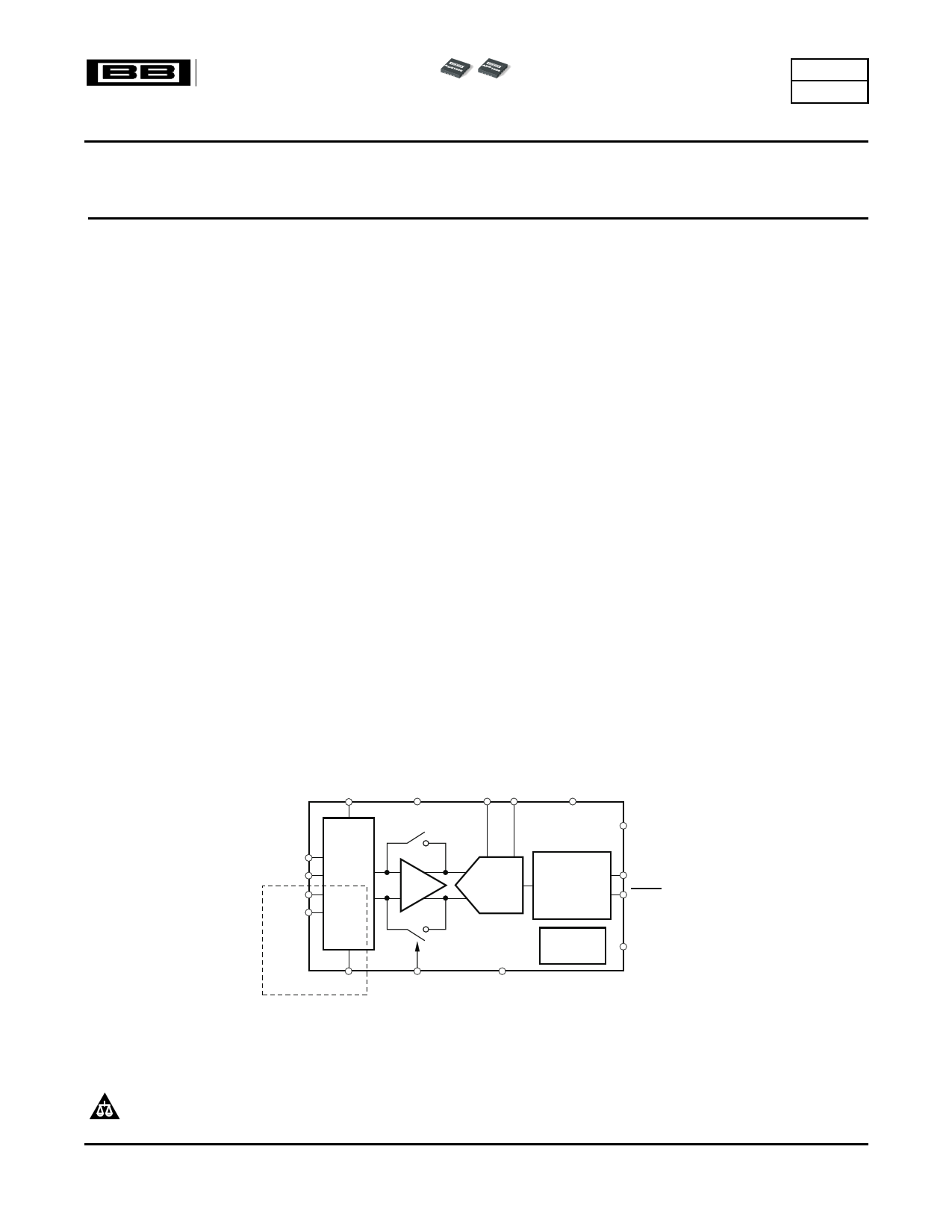
TEMPEN
AVDD
DESCRIPTION
The ADS1225 and ADS1226 are 24-bit delta-sigma
analog-to-digital (A/D) converters. They offer
excellent performance, ease-of-use, and low power
in a small 4mm × 4mm QFN package and are
well-suited for demanding high-resolution
measurements, especially in portable and other
space-saving and power-constrained applications.
The ADS1225 and ADS1226 convert on command
using a dedicated START pin. Simply pulse this pin
to initiate a conversion. Data is read in a single cycle
for retrieval over a 2-wire serial interface that easily
connects to popular microcontrollers like the
MSP430. After the conversion completes, the
ADS1225 and ADS1226 automatically shuts down all
circuitry.
Internal features include a two-channel multiplexer
(ADS1226), selectable input buffer, temperature
sensor, and oscillator. The full-scale range is defined
by the external voltage reference with support
provided for up to a 5V differential input signal. Two
operating modes allow for speed (100SPS data rate,
15µVRMS noise) or resolution (4µVRMS noise, 16SPS
data rate).
The ADS1225/6 supports 2.7 to 5.5V analog and
digital supplies. Power consumption is 1mW while
converting with 3V supplies. The ADS1225 and
ADS1226 are fully specified over an extended
industrial temperature range of –40°C to +105°C.
VREFP VREFN DVDD
AINP1
AINN1
AINP2
AINN2
MUX
Buffer
START
DS
ADC
Serial Interface
SCLK
DRDY/DOUT
Oscillator
MODE
MUX
ADS1226 Only
BUFEN
GND
Please be aware that an important notice concerning availability, standard warranty, and use in critical applications of Texas
Instruments semiconductor products and disclaimers thereto appears at the end of this data sheet.
All trademarks are the property of their respective owners.
PRODUCTION DATA information is current as of publication date.
Products conform to specifications per the terms of the Texas
Instruments standard warranty. Production processing does not
necessarily include testing of all parameters.
Copyright © 2006, Texas Instruments Incorporated
1 page 
www.ti.com
PIN CONFIGURATION
RGV PACKAGE
QFN-16 4.0mm x 4.0mm
(TOP VIEW)
ADS1225
ADS1226
SBAS346 – MAY 2006
START 1
SCLK 2
DRDY/DOUT 3
BUFEN 4
ADS1225
12 GND
11 AINN1
10 AINP1
9 NC
NAME
START
SCLK
TERMINAL
NO.
1
2
DRDY/DOUT
3
BUFEN
GND
TEMPEN
MODE
NC
NC
AINP1
AINN1
GND
VREFN
VREFP
AVDD
DVDD
4
5
6
7
8
9
10
11
12
13
14
15
16
PIN DESCRIPTIONS – ADS1225
ANALOG/DIGITAL
INPUT/OUTPUT
Digital Input
Digital Input
Digital Output
Digital Input
Ground
Digital Input
Digital Input
Analog Input
Analog Input
Ground
Analog Input
Analog Input
Analog
Digital
DESCRIPTION
High: Start conversions; Low: Shutdown
Serial clock input
Dual-purpose output:
Data ready: indicates valid data by going low.
Data output: outputs data, MSB first, on the rising edge of SCLK.
Enables buffer after MUX
Ground
Selects temperature sensor input from MUX
Selects between High-Speed and High-Resolution modes
No connect
No connect
Analog channel 1 positive input
Analog channel 1 negative input
Analog and digital ground
Negative reference input
Positive reference input
Analog power supply
Digital power supply
Submit Documentation Feedback
5
5 Page 
www.ti.com
Analog Input Measurement Without the Input
Buffer
With the buffer disabled by setting the BUFEN pin
low, the ADS1225 and ADS1226 measure the input
signal using internal capacitors that are continuously
charged and discharged. Figure 20 shows a
simplified schematic of the ADS1225/6 input circuitry,
with Figure 21 showing the on/off timings of the
switches. The S1 switches close during the input
sampling phase. With S1 closed, CA1 charges to
AINP, CA2 charges to AINN, and CB charges to
(AINP – AINN). For the discharge phase, S1 opens
first and then S2 closes. CA1 and CA2 discharge to
approximately VDD/2 and CB discharges to 0V. The
constant charging of the input capacitors presents a
load on the inputs that can be represented by
effective impedances. Figure 22 shows the input
circuitry with the capacitors and switches of
Figure 20 by their effective impedances.
AINPx
AINNx
ESD Protection
AVDD
AVDD
AVDD/2
AINP S1
MUX
AINN S1
S2
S2
AVDD/2
CA1
3pF
CB
6pF
CA2
3pF
Figure 20. Simplified Input Structure with the
Buffer Turned Off
ON
S1
OFF
ON
S2
OFF
tSAMPLE = 12ms
Figure 21. S1 and S2 Switch Timing for Figure 20
ADS1225
ADS1226
SBAS346 – MAY 2006
AINPx
AINNx
AVDD/2
ZeffA = tSAMPLE/CA1 = 4MW
ZeffB = tSAMPLE/CB = 2MW
ZeffA = tSAMPLE/CA2 = 4MW
AVDD/2
Figure 22. Effective Analog Input Impedances
with the Buffer Off
ESD silicon diodes protect the inputs. To keep these
diodes from turning on, make sure the voltages on
the input pins do not go below GND by more than
100mV, and likewise do not exceed VDD by 100mV.
This limitation is shown in Equation 1:
GND * 100mV t (AINP, AINN) t VDD ) 100mV
(1)
Analog Input Measurement with the Input Buffer
When the buffer is enabled by setting the BUFEN pin
high, a low-drift, chopper-stabilized input buffer is
used to achieve very high input impedance. The
buffer charges the input sampling capacitors, thus
removing the load from the measurement. Because
the input buffer is chopper-stabilized, the charging of
parasitic capacitances causes the charge to be
carried away, as if by resistance. The input
impedance can be modeled by a single resistor, as
shown in Figure 23.
AINP
AINN
1GW
Figure 23. Effective Analog Input Impedances
with the Buffer On
Note that the analog inputs (listed in the Electrical
Characteristics table as Absolute Input Range) must
remain between GND + 0.05V to AVDD – 1.5V.
Exceeding this range degrades linearity and results
in performance outside the specified limits.
Submit Documentation Feedback
11
11 Page | ||
| Páginas | Total 24 Páginas | |
| PDF Descargar | [ Datasheet ADS1225.PDF ] | |
Hoja de datos destacado
| Número de pieza | Descripción | Fabricantes |
| ADS1220 | ADS1220 Low-Power Low-Noise 24-Bit ADC for Small-Signal Sensors (Rev. B) | Texas Instruments |
| ADS1222 | 24 BIT ANALOG TO DIGITAL CONVERTER WITH 2-CHANNEL DIFFERENTIAL INPUT MULTIPLEXER | Burr-Brown Corporation |
| ADS1222 | ADS1222: 24-Bit A/D Conv with 2-Channel Differential Input Multiplexer (Rev. B) | Texas Instruments |
| ADS1222IPWR | 24 BIT ANALOG TO DIGITAL CONVERTER WITH 2-CHANNEL DIFFERENTIAL INPUT MULTIPLEXER | Burr-Brown Corporation |
| Número de pieza | Descripción | Fabricantes |
| SLA6805M | High Voltage 3 phase Motor Driver IC. |
Sanken |
| SDC1742 | 12- and 14-Bit Hybrid Synchro / Resolver-to-Digital Converters. |
Analog Devices |
|
DataSheet.es es una pagina web que funciona como un repositorio de manuales o hoja de datos de muchos de los productos más populares, |
| DataSheet.es | 2020 | Privacy Policy | Contacto | Buscar |