|
|
|
PDF 56F803 Data sheet ( Hoja de datos )
| Número de pieza | 56F803 | |
| Descripción | 16-bit Hybrid Controller | |
| Fabricantes | Motorola Semiconductors | |
| Logotipo | ||
Hay una vista previa y un enlace de descarga de 56F803 (archivo pdf) en la parte inferior de esta página. Total 48 Páginas | ||
|
No Preview Available !
www.DataSheet4U.com
Freescale Semiconductor, Inc.
DSP56F803/D
Rev. 13.0, 02/2004
56F803
Technical Data
56F803 16-bit Hybrid Controller
• Up to 40 MIPS at 80MHz core frequency
• DSP and MCU functionality in a unified,
C-efficient architecture
• Up to 64K × 16-bit words each of external
Program and Data memory
• 6-channel PWM module
• Hardware DO and REP loops
• Two 4-channel 12-bit ADCs
• MCU-friendly instruction set supports both
DSP and controller functions: MAC, bit
manipulation unit, 14 addressing modes
• 31.5K × 16-bit words Program Flash
• 512 × 16-bit words Program RAM
• 4K × 16-bit words Data Flash
• 2K × 16-bit words Data RAM
• 2K × 16-bit words Boot Flash
• Quadrature Decoder
• CAN 2.0 B module
• Serial Communication Interface (SCI)
• Serial Peripheral Interface (SPI)
• Up to two General Purpose Quad Timers
• JTAG/OnCETM port for debugging
• 16 shared GPIO lines
• 100–pin LQFP package
6
PWM Outputs
Current Sense Inputs
3
Fault Inputs
3
PWMA
EXTBOOT
RESET
IRQB
IRQA
6
VCAPC VDD VSS VDDA
26
6*
VSSA
A/D1
4 A/D2 ADC
4 VREF
Quadrature
Decoder 0 /
4 Quad Timer A
Interrupt
Controller
JTAG/
OnCE
Port
Digital Reg Analog Reg
Low Voltage
Supervisor
Program Controller
and
Hardware Looping Unit
Address
Generation
Unit
Data ALU
16 x 16 + 36 → 36-Bit MAC
Three 16-bit Input Registers
Two 36-bit Accumulators
Bit
Manipulation
Unit
Program Memory
32252 x 16 Flash
• • •512 x 16 SRAM
PAB
PDB
16-Bit
PLL
CLKO
Quad Timer B
Boot Flash
56800
XTAL
Quad Timer C
2048 x 16 Flash
XDB2
Core
Clock Gen
EXTAL
Quad Timer D
Data Memory
4096 x 16 Flash
2 2048 x 16 SRAM
CAN 2.0A/B
2
SCI
or
2 GPIO
COP/
CGDB
• • •XAB1
•XAB2
•INTERRUPT
IPBB
CONTROLS CONTROLS
16 16
External 6
Address Bus
A[00:05]
A[06:15] or
4
SPI
or
GPIO
Watchdog
Application-
Specific
Memory &
COP RESET
MODULE CONTROLS
ADDRESS BUS [8:0]
DATA BUS [15:0]
IPBus Bridge
(IPBB)
External
Bus
Interface
Unit
Switch
External
Data Bus
Switch
Bus
GPIO-E2:E3 &
10 GPIO-A0:A7
D[00:15]
16
PS Select
DS Select
Peripherals
Control
WR Enable
*includes TCS pin which is reserved for factory use and is tied to VSS
RD Enable
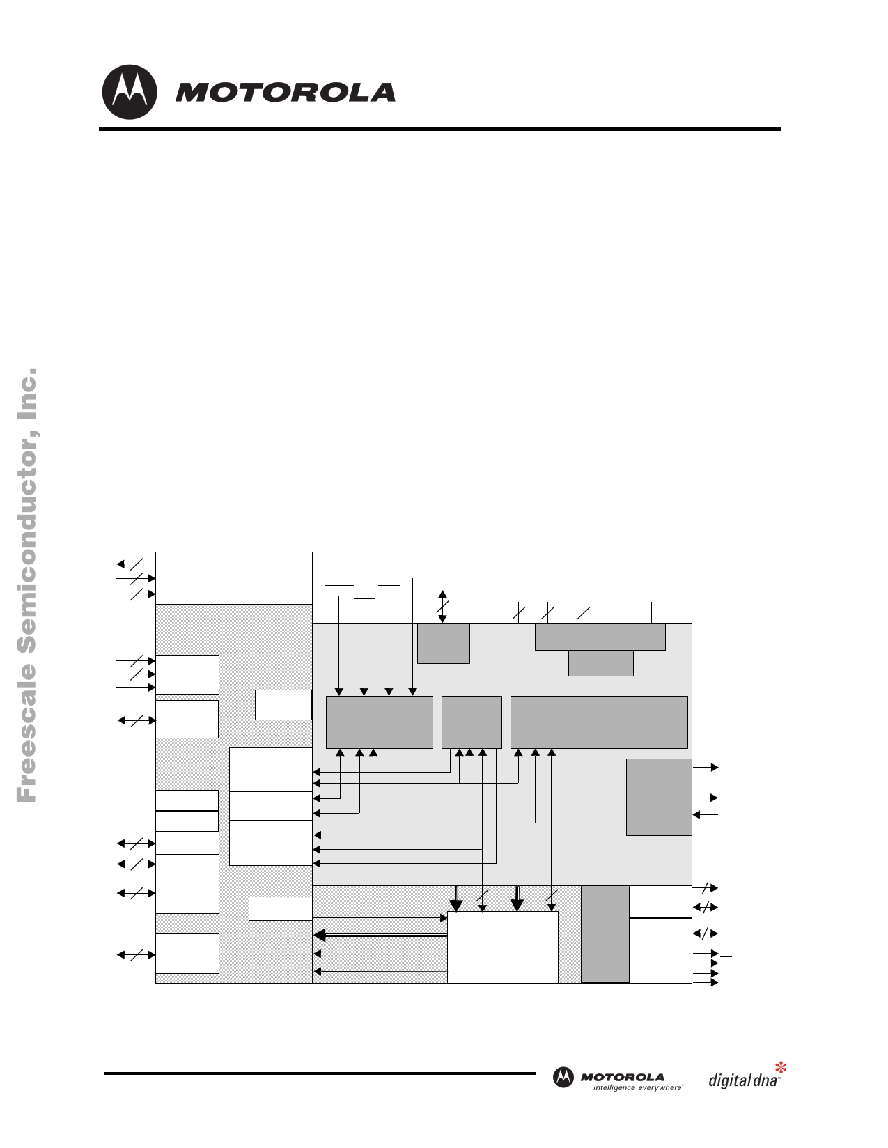
Figure 1. 56F803 Block Diagram
© Motorola, Inc., 2004. All rights reserved.
For More Information On This Product,
Go to: www.freescale.com
1 page 
www.DataSheet4U.com
Freescale Semiconductor, Inc.
Product Documentation
1.4 Product Documentation
The four documents listed in Table 1 are required for a complete description and proper design with the
56F803. Documentation is available from local Motorola distributors, Motorola semiconductor sales
offices, Motorola Literature Distribution Centers, or online at www.motorola.com/semiconductors.
Table 1. 56F803 Chip Documentation
Topic
Description
Order Number
DSP56800
Family Manual
DSP56F801/803/805/
807 User’s Manual
56F803
Technical Data Sheet
56F803
Product Brief
Detailed description of the 56800 family architecture, and
16-bit core processor and the instruction set
DSP56800FM/D
Detailed description of memory, peripherals, and interfaces DSP56F801-7UM/D
of the 56F801, 56F803, 56F803, and 56F807
Electrical and timing specifications, pin descriptions, and
package descriptions (this document)
DSP56F803/D
Summary description and block diagram of the 56F803 core, DSP56F803PB/D
memory, peripherals and interfaces
56F803
Errata
Details any chip issues that might be present
DSP56F803E/D
1.5 Data Sheet Conventions
This data sheet uses the following conventions:
OVERBAR
This is used to indicate a signal that is active when pulled low. For example, the RESET pin is
active when low.
“asserted”
A high true (active high) signal is high or a low true (active low) signal is low.
“deasserted” A high true (active high) signal is low or a low true (active low) signal is high.
Examples:
Signal/Symbol
Logic State
Signal State
Voltage1
PIN
True
Asserted
VIL/VOL
PIN
False
Deasserted
VIH/VOH
PIN
True
Asserted
VIH/VOH
PIN
False
Deasserted
1. Values for VIL, VOL, VIH, and VOH are defined by individual product specifications.
VIL/VOL
56F803 Technical Data
For More Information On This Product,
Go to: www.freescale.com
5
5 Page 
www.DataSheet4U.com
Freescale Semiconductor, Inc.
Pulse Width Modulator (PWM) Signals
Table 10. Interrupt and Program Control Signals (Continued)
No. of
Pins
Signal
Name
Signal
Type
State During
Reset
Signal Description
1 RESET Input
(Schmitt)
1 EXTBOOT Input
(Schmitt)
Input
Input
Reset—This input is a direct hardware reset on the
processor. When RESET is asserted low, the hybrid
controller is initialized and placed in the Reset state. A
Schmitt trigger input is used for noise immunity. When the
RESET pin is deasserted, the initial chip operating mode is
latched from the EXTBOOT pin. The internal reset signal will
be deasserted synchronous with the internal clocks, after a
fixed number of internal clocks.
To ensure a complete hardware reset, RESET and TRST
should be asserted together. The only exception occurs in a
debugging environment when a hardware device reset is
required and it is necessary not to reset the OnCE/JTAG
module. In this case, assert RESET, but do not assert TRST.
External Boot—This input is tied to VDD to force device to
boot from off-chip memory. Otherwise, it is tied to VSS.
2.6 Pulse Width Modulator (PWM) Signals
Table 11. Pulse Width Modulator (PWMA) Signals
No. of
Pins
Signal
Name
Signal State During
Type
Reset
Signal Description
6 PWMA0–5 Output Tri-stated PWMA0–5— These are six PWMA output pins.
3 ISA0–2 Input
Input
ISA0–2— These three input current status pins are used for
(Schmitt)
top/bottom pulse width correction in complementary channel
operation for PWMA.
3 FAULTA0–2 Input
(Schmitt)
Input
FAULTA0–2— These three fault input pins are used for
disabling selected PWMA outputs in cases where fault
conditions originate off-chip.
56F803 Technical Data
For More Information On This Product,
Go to: www.freescale.com
11
11 Page | ||
| Páginas | Total 48 Páginas | |
| PDF Descargar | [ Datasheet 56F803.PDF ] | |
Hoja de datos destacado
| Número de pieza | Descripción | Fabricantes |
| 56F801 | 16-bit Hybrid Controller | Motorola Semiconductors |
| 56F801 | 16-bit Digital Signal Controllers | Freescale Semiconductor |
| 56F8011 | (56F8011 / 56F8013) 16-Bit Digital Signal Controller | Motorola Semiconductor |
| 56F8013 | 16-bit Digital Signal Controllers | Freescale Semiconductor |
| Número de pieza | Descripción | Fabricantes |
| SLA6805M | High Voltage 3 phase Motor Driver IC. |
Sanken |
| SDC1742 | 12- and 14-Bit Hybrid Synchro / Resolver-to-Digital Converters. |
Analog Devices |
|
DataSheet.es es una pagina web que funciona como un repositorio de manuales o hoja de datos de muchos de los productos más populares, |
| DataSheet.es | 2020 | Privacy Policy | Contacto | Buscar |