|
|
|
PDF AD9219 Data sheet ( Hoja de datos )
| Número de pieza | AD9219 | |
| Descripción | 40/65 MSPS Serial LVDS 1.8 V A/D Converter | |
| Fabricantes | Analog Devices | |
| Logotipo | ||
Hay una vista previa y un enlace de descarga de AD9219 (archivo pdf) en la parte inferior de esta página. Total 30 Páginas | ||
|
No Preview Available !
Data Sheet
FEATURES
4 ADCs integrated into 1 package
94 mW ADC power per channel at 65 MSPS
SNR = 60 dB (to Nyquist)
ENOB = 9.7 bits
SFDR = 78 dBc (to Nyquist)
Excellent linearity
DNL = ±0.2 LSB (typical)
INL = ±0.3 LSB (typical)
Serial LVDS (ANSI-644, default)
Low power, reduced signal option (similar to IEEE 1596.3)
Data and frame clock outputs
315 MHz full-power analog bandwidth
2 V p-p input voltage range
1.8 V supply operation
Serial port control
Full-chip and individual-channel power-down modes
Flexible bit orientation
Built-in and custom digital test pattern generation
Programmable clock and data alignment
Programmable output resolution
Standby mode
APPLICATIONS
Medical imaging and nondestructive ultrasound
Portable ultrasound and digital beam-forming systems
Quadrature radio receivers
Diversity radio receivers
Tape drives
Optical networking
Test equipment
GENERAL DESCRIPTION
The AD9219 is a quad, 10-bit, 40/65 MSPS analog-to-digital con-
verter (ADC) with an on-chip sample-and-hold circuit designed
for low cost, low power, small size, and ease of use. The product
operates at a conversion rate of up to 65 MSPS and is optimized for
outstanding dynamic performance and low power in applications
where a small package size is critical.
The ADC requires a single 1.8 V power supply and LVPECL-/
CMOS-/LVDS-compatible sample rate clock for full performance
operation. No external reference or driver components are
required for many applications.
Rev. E
Information furnished by Analog Devices is believed to be accurate and reliable. However, no
responsibility is assumed by Analog Devices for its use, nor for any infringements of patents or other
rights of third parties that may result from its use. Specifications subject to change without notice. No
license is granted by implication or otherwise under any patent or patent rights of Analog Devices.
Trademarksandregisteredtrademarksarethepropertyoftheirrespectiveowners.
Quad, 10-Bit, 40/65 MSPS
Serial LVDS 1.8 V ADC
AD9219
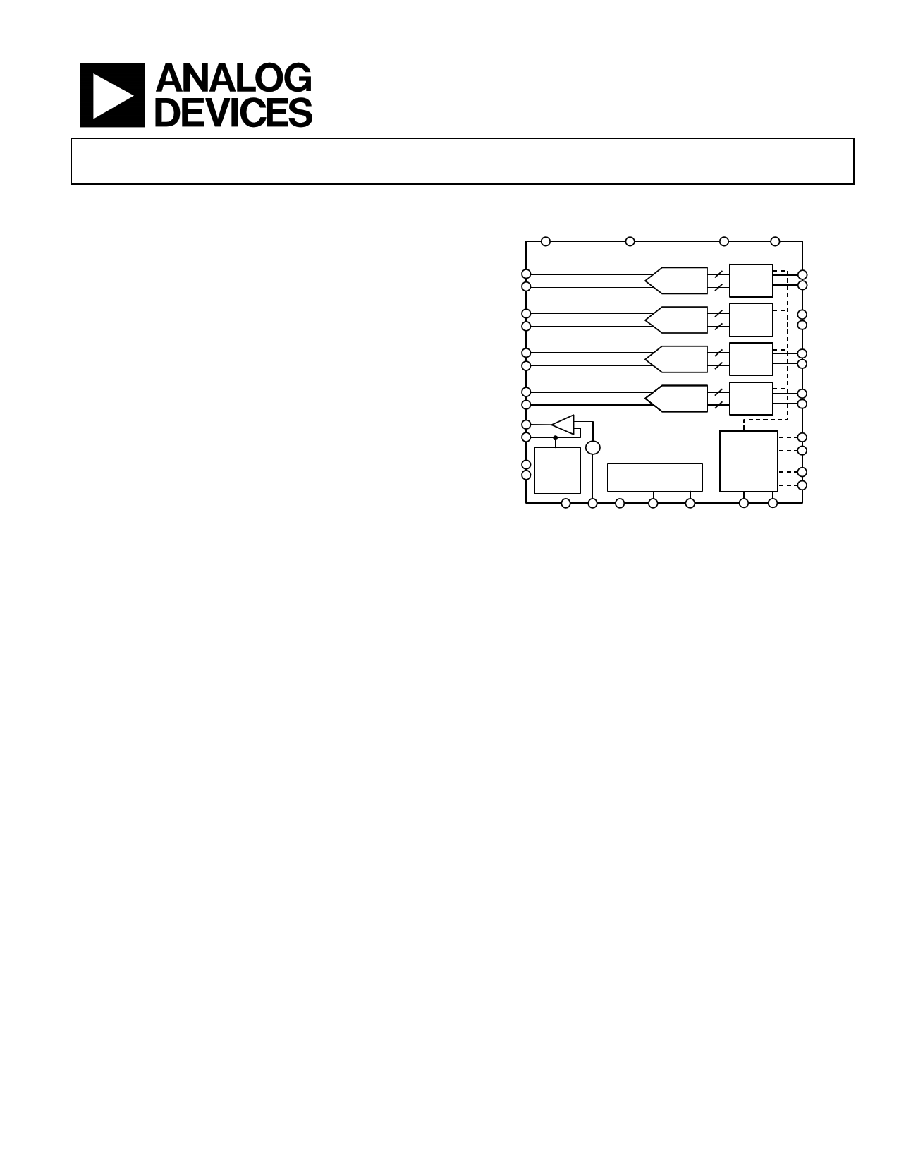
FUNCTIONAL BLOCK DIAGRAM
AVDD
PDWN
DRVDD DRGND
VIN + A
VIN – A
VIN + B
VIN – B
VIN + C
VIN – C
VIN + D
VIN – D
VREF
SENSE
REFT
REFB
AD9219
10
PIPELINE
ADC
SERIAL
LVDS
10
PIPELINE
SERIAL
ADC
LVDS
10
PIPELINE
SERIAL
ADC
LVDS
10
PIPELINE
SERIAL
ADC
LVDS
REF
SELECT
+– 0.5V
SERIAL PORT
INTERFACE
DATA RATE
MULTIPLIER
D+A
D–A
D+B
D–B
D+C
D–C
D+D
D–D
FCO+
FCO–
DCO+
DCO–
RBIAS AGND CSB SDIO/ODM SCLK/DTP CLK+ CLK–
Figure 1.
The ADC automatically multiplies the sample rate clock for the
appropriate LVDS serial data rate. A data clock output (DCO) for
capturing data on the output and a frame clock output (FCO)
for signaling a new output byte are provided. Individual-channel
power-down is supported and typically consumes less than
2 mW when all channels are disabled.
The ADC contains several features designed to maximize
flexibility and minimize system cost, such as programmable
clock and data alignment and programmable digital test pattern
generation. The available digital test patterns include built-in
deterministic and pseudorandom patterns, along with custom user-
defined test patterns entered via the serial port interface (SPI).
The AD9219 is available in an RoHS compliant, 48-lead LFCSP. It is
specified over the industrial temperature range of −40°C to +85°C.
PRODUCT HIGHLIGHTS
1. Small Footprint. Four ADCs are contained in a small, space-
saving package.
2. Low power of 94 mW/channel at 65 MSPS.
3. Ease of Use. A data clock output (DCO) is provided that
operates at frequencies of up to 390 MHz and supports
double data rate (DDR) operation.
4. User Flexibility. The SPI control offers a wide range of flexible
features to meet specific system requirements.
5. Pin-Compatible Family. This includes the AD9287 (8-bit),
AD9228 (12-bit), and AD9259 (14-bit).
One Technology Way, P.O. Box 9106, Norwood, MA 02062-9106, U.S.A.
Tel: 781.329.4700
www.analog.com
Fax: 781.461.3113 ©2006–2011 Analog Devices, Inc. All rights reserved.
1 page 
AD9219
Data Sheet
SPECIFICATIONS
AVDD = 1.8 V, DRVDD = 1.8 V, 2 V p-p differential input, 1.0 V internal reference, AIN = −0.5 dBFS, unless otherwise noted.
Table 1.
Parameter1
RESOLUTION
ACCURACY
No Missing Codes
Offset Error
Offset Matching
Gain Error
Gain Matching
Differential Nonlinearity (DNL)
Integral Nonlinearity (INL)
TEMPERATURE DRIFT
Offset Error
Gain Error
Reference Voltage (1 V Mode)
REFERENCE
Output Voltage Error (VREF = 1 V)
Load Regulation at 1.0 mA (VREF = 1 V)
Input Resistance
ANALOG INPUTS
Differential Input Voltage (VREF = 1 V)
Common-Mode Voltage
Differential Input Capacitance
Analog Bandwidth, Full Power
POWER SUPPLY
AVDD
DRVDD
IAVDD
IDRVDD
Total Power Dissipation (Including Output Drivers)
Power-Down Dissipation
Standby Dissipation2
CROSSTALK
CROSSTALK (Overrange Condition)3
Temperature
Full
Full
Full
Full
Full
Full
Full
Full
Full
Full
Full
Full
Full
Full
Full
Full
Full
Full
Full
Full
Full
Full
Full
Full
Full
Full
AD9219-40
Min Typ
Max
10
AD9219-65
Min Typ
Max
10
Unit
Bits
Guaranteed
±1 ±8
±2 ±8
±0.4 ±1.2
±0.3 ±0.7
±0.1 ±0.4
±0.15 ±0.4
Guaranteed
±1 ±8
±2 ±8
±2 ±3.5
±0.3 ±0.7
±0.15 ±0.4
±0.3 ±0.75
mV
mV
% FS
% FS
LSB
LSB
±2 ±2 ppm/°C
±17 ±17 ppm/°C
±21 ±21 ppm/°C
±2 ±30
3
6
±2 ±30 mV
3 mV
6 kΩ
2
AVDD/2
7
315
2
AVDD/2
7
315
V p-p
V
pF
MHz
1.7 1.8
1.7 1.8
130
30
295
2
72
−100
−100
1.9 1.7 1.8
1.9 1.7 1.8
142 177
32 33
313 378
5.8 2
72
−100
−100
1.9 V
1.9 V
190 mA
37 mA
408 mW
5.8 mW
mW
dB
dB
1 See the AN-835 Application Note, Understanding High Speed ADC Testing and Evaluation, for definitions and for details of how these tests were completed.
2 Can be controlled via the SPI.
3 Overrange condition is specific with 6 dB of the full-scale input range.
Rev. E | Page 4 of 56
5 Page 
AD9219
ABSOLUTE MAXIMUM RATINGS
Table 5.
Parameter
ELECTRICAL
AVDD
DRVDD
AGND
AVDD
Digital Outputs
(D + x, D − x, DCO+,
DCO−, FCO+, FCO−)
CLK+, CLK−
VIN + x, VIN − x
SDIO/ODM
PDWN, SCLK/DTP, CSB
REFT, REFB, RBIAS
VREF, SENSE
ENVIRONMENTAL
Operating Temperature
Range (Ambient)
Maximum Junction
Temperature
Lead Temperature
(Soldering, 10 sec)
Storage Temperature
Range (Ambient)
With
Respect To Rating
AGND
DRGND
DRGND
DRVDD
DRGND
−0.3 V to +2.0 V
−0.3 V to +2.0 V
−0.3 V to +0.3 V
−2.0 V to +2.0 V
−0.3 V to +2.0 V
AGND
AGND
AGND
AGND
AGND
AGND
−0.3 V to +3.9 V
−0.3 V to +2.0 V
−0.3 V to +2.0 V
−0.3 V to +3.9 V
−0.3 V to +2.0 V
−0.3 V to +2.0 V
−40°C to +85°C
150°C
300°C
−65°C to +150°C
Data Sheet
Stresses above those listed under Absolute Maximum Ratings
may cause permanent damage to the device. This is a stress
rating only; functional operation of the device at these or any
other conditions above those indicated in the operational
section of this specification is not implied. Exposure to absolute
maximum rating conditions for extended periods may affect
device reliability.
THERMAL IMPEDANCE
Table 6.
Air Flow Velocity (m/sec)
0.0
1.0
2.5
θJA1
θJB
θJC Unit
24 °C/W
21 12.6 1.2 °C/W
19 °C/W
1 θJA for a 4-layer PCB with solid ground plane (simulated). Exposed pad
soldered to PCB.
ESD CAUTION
Rev. E | Page 10 of 56
11 Page | ||
| Páginas | Total 30 Páginas | |
| PDF Descargar | [ Datasheet AD9219.PDF ] | |
Hoja de datos destacado
| Número de pieza | Descripción | Fabricantes |
| AD9211 | 1.8 V Analog-to-Digital Converter | Analog Devices |
| AD9212 | Serial LVDS A/D Converter | Analog Devices |
| AD9214 | 3V A/D Converter | Analog Devices |
| AD9215 | 3V A/D Converter | Analog Devices |
| Número de pieza | Descripción | Fabricantes |
| SLA6805M | High Voltage 3 phase Motor Driver IC. |
Sanken |
| SDC1742 | 12- and 14-Bit Hybrid Synchro / Resolver-to-Digital Converters. |
Analog Devices |
|
DataSheet.es es una pagina web que funciona como un repositorio de manuales o hoja de datos de muchos de los productos más populares, |
| DataSheet.es | 2020 | Privacy Policy | Contacto | Buscar |