|
|
PDF HY5DU56822DT Data sheet ( Hoja de datos )
| Número de pieza | HY5DU56822DT | |
| Descripción | (HY5DU56xx22DT) 256Mb DDR SDRAM | |
| Fabricantes | Hynix Semiconductor | |
| Logotipo | ||
Hay una vista previa y un enlace de descarga de HY5DU56822DT (archivo pdf) en la parte inferior de esta página. Total 29 Páginas | ||
|
No Preview Available !
www.DataSheet4U.com
256Mb DDR SDRAM
256Mb DDR SDRAM
HY5DU56422D(L)T
HY5DU56822D(L)T
HY5DU561622D(L)T
This document is a general product description and is subject to change without notice. Hynix Semiconductor does not assume any
responsibility for use of circuits described. No patent licenses are implied.
Rev. 1.0 /Oct. 2004
1
1 page 
www.DataSheet4U.com
HY5DU56422D(L)T
HY5DU56822D(L)T
HY5DU561622D(L)T
PIN DESCRIPTION
PIN TYPE
CK, /CK
Input
CKE Input
/CS
BA0, BA1
Input
Input
A0 ~ A12
Input
/RAS, /CAS, /
WE
DM
(LDM,UDM)
Input
Input
DQS
(LDQS,UDQS)
I/O
DQ
VDD/VSS
VDDQ/VSSQ
VREF
NC
I/O
Supply
Supply
Supply
NC
Rev. 1.0 /Oct. 2004
DESCRIPTION
Clock: CK and /CK are differential clock inputs. All address and control input sig-
nals are sampled on the crossing of the positive edge of CK and negative edge of
/CK. Output (read) data is referenced to the crossings of CK and /CK (both direc-
tions of crossing).
Clock Enable: CKE HIGH activates, and CKE LOW deactivates internal clock sig-
nals, and device input buffers and output drivers. Taking CKE LOW provides PRE-
CHARGE POWER DOWN and SELF REFRESH operation (all banks idle), or ACTIVE
POWER DOWN (row ACTIVE in any bank). CKE is synchronous for POWER
DOWN entry and exit, and for SELF REFRESH entry. CKE is asynchronous for
SELF REFRESH exit, and for output disable. CKE must be maintained high
throughout READ and WRITE accesses. Input buffers, excluding CK, /CK and
CKE are disabled during POWER DOWN. Input buffers, excluding CKE are dis-
abled during SELF REFRESH. CKE is an SSTL_2 input, but will detect an LVCMOS
LOW level after VDD is applied.
Chip Select: Enables or disables all inputs except CK, /CK, CKE, DQS and DM. All
commands are masked when CS is registered high. CS provides for external bank
selection on systems with multiple banks. CS is considered part of the command
code.
Bank Address Inputs: BA0 and BA1 define to which bank an ACTIVE, Read, Write
or PRECHARGE command is being applied.
Address Inputs: Provide the row address for ACTIVE commands, and the column
address and AUTO PRECHARGE bit for READ/WRITE commands, to select one
location out of the memory array in the respective bank. A10 is sampled during a
precharge command to determine whether the PRECHARGE applies to one bank
(A10 LOW) or all banks (A10 HIGH). If only one bank is to be precharged, the
bank is selected by BA0, BA1. The address inputs also provide the op code dur-
ing a MODE REGISTER SET command. BA0 and BA1 define which mode register
is loaded during the MODE REGISTER SET command (MRS or EMRS).
Command Inputs: /RAS, /CAS and /WE (along with /CS) define the command
being entered.
Input Data Mask: DM is an input mask signal for write data. Input data is masked
when DM is sampled HIGH along with that input data during a WRITE access.
DM is sampled on both edges of DQS. Although DM pins are input only, the DM
loading matches the DQ and DQS loading. For the x16, LDM corresponds to the
data on DQ0-Q7; UDM corresponds to the data on DQ8-Q15.
Data Strobe: Output with read data, input with write data. Edge aligned with
read data, centered in write data. Used to capture write data. For the x16, LDQS
corresponds to the data on DQ0-Q7; UDQS corresponds to the data on DQ8-
Q15.
Data input / output pin: Data bus
Power supply for internal circuits and input buffers.
Power supply for output buffers for noise immunity.
Reference voltage for inputs for SSTL interface.
No connection.
5
5 Page 
www.DataSheet4U.com
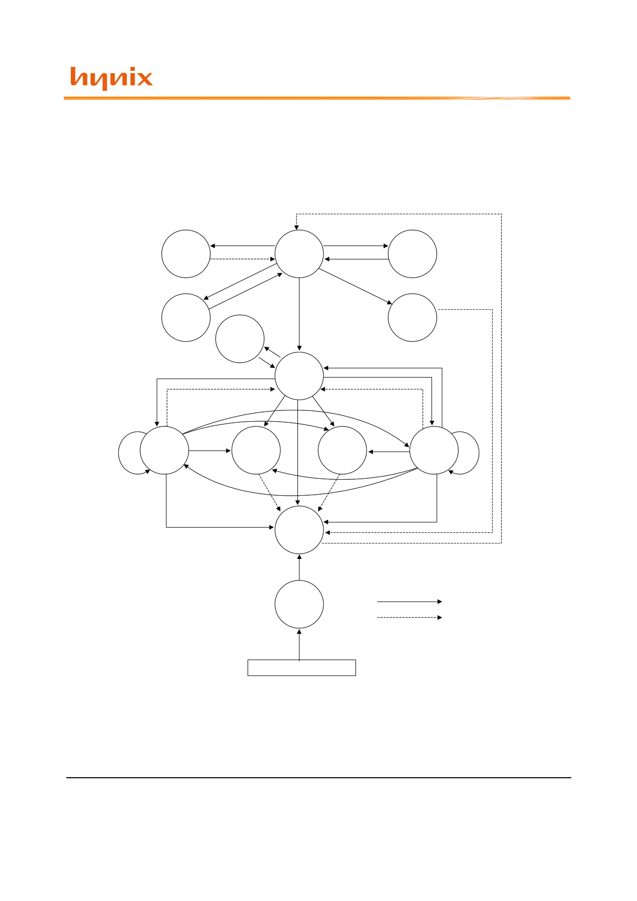
SIMPLIFIED STATE DIAGRAM
HY5DU56422D(L)T
HY5DU56822D(L)T
HY5DU561622D(L)T
MODE
REGISTER
SET
MRS
PDEN
IDLE
POWER
DOWN
PDEX
ACT
POWER
DOWN
PDEN
PDEX
BANK
ACTIVE
SREF
SREX
AREF
SELF
REFRESH
AUTO
REFRESH
BST
WRITE
WRITE
READ
READAP
WRITEAP
WRITE
WITH
AUTOPRE-
CHARGE
READ
WITH READAP
AUTOPRE-
CHARGE WRITEAP
READ
READ
PRE(PALL)
PRE-
CHARGE
WRITE
PRE(PALL)
POWER-UP
POWER APPLIED
Command Input
Automatic Sequence
Rev. 1.0 /Oct. 2004
11
11 Page | ||
| Páginas | Total 29 Páginas | |
| PDF Descargar | [ Datasheet HY5DU56822DT.PDF ] | |
Hoja de datos destacado
| Número de pieza | Descripción | Fabricantes |
| HY5DU56822DT | (HY5DU56xx22DT) 256Mb DDR SDRAM | Hynix Semiconductor |
| HY5DU56822DTP | (HY5DU56x22DTP) 256M DDR SDRAM | Hynix Semiconductor |
| Número de pieza | Descripción | Fabricantes |
| SLA6805M | High Voltage 3 phase Motor Driver IC. |
Sanken |
| SDC1742 | 12- and 14-Bit Hybrid Synchro / Resolver-to-Digital Converters. |
Analog Devices |
|
DataSheet.es es una pagina web que funciona como un repositorio de manuales o hoja de datos de muchos de los productos más populares, |
| DataSheet.es | 2020 | Privacy Policy | Contacto | Buscar |
