|
|
PDF HCD66740 Data sheet ( Hoja de datos )
| Número de pieza | HCD66740 | |
| Descripción | 112 x 80-dot Graphics LCD Controller/Driver | |
| Fabricantes | Hitachi Semiconductor | |
| Logotipo | ||
Hay una vista previa y un enlace de descarga de HCD66740 (archivo pdf) en la parte inferior de esta página. Total 30 Páginas | ||
|
No Preview Available !
www.DataSheet4U.com
HD66740
HD66740
(112 x 80-dot Graphics LCD Controller/Driver)
Rev 1.0
August, 2001
Description
The HD66740, 112-by-80 dot-matrix graphics LCD controller and driver LSI, displays graphics such as
text, kanji and pictograms. It can be configured to drive a dot-matrix liquid crystal under the control of the
microprocessor connected via the clock-synchronized serial or 4/8-bit bus. The HD66740 has a smooth
vertical scroll display and a double-height display for the remaining bit map areas. It fixed-displays a part
of the graphics icons so that the user can easily see a variety of information.
The HD66740 has various functions to reduce the power consumption of an LCD system such as low-
voltage operation of 1.8 V min., a booster to generate maximum five-times LCD drive voltage from the
supplied voltage, and voltage-followers to decrease the direct current flow in the LCD drive bleeder-
resistors. Combining these hardware functions with software functions such as standby and sleep modes
allows fine power control. The HD66740 is suitable for any portable battery-driven product requiring
long-term driving capabilities such as cellular phones, pagers, or electronic wallets.
Features
• Control and drive of a graphics LCD
• 112 x 80-dot display
• Fixed display of graphics icons (pictograms)
• Low-power operation support:
Vcc = 1.8 to 3.6 V (low voltage)
VLCD = 4.5 to 15.0 V (liquid crystal drive voltage)
Triple, quadruple, or five-times booster for liquid crystal drive voltage
64-step contrast adjuster and voltage followers to decrease direct current flow in the LCD drive
bleeder-resistors
Power-save functions such as the standby mode and sleep mode supported
Programmable drive duty ratios and bias values displayed on LCD
• High-speed clock-synchronized serial interface (serial transfer rate: 5 MHz max.)
• I2C bus interface
• High-speed 4-/8-bit bus interface capability
• 112-segment × 80-common liquid crystal display driver
• 1,120-byte (112 × 80 dots) character generator RAM
1
1 page 
www.DataSheet4U.com
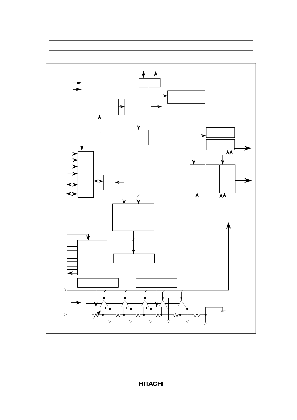
HD66740 Block Diagram
RESET*
TEST
Instruction register
(IR)
OSC1 OSC2
CPG
Instruction
decoder
Timing generator
HD66740
8
IM2-1
IM0/ID
CS*
RS
E/WR*/SCL
RW/RD*/SDA
DB0-DB7
System
interface
- Clock
synchro-
nized
serial
8 Data
- I2C bus
register
- 4-bit bus
(DR)
- 8-bit bus
Address
counter
(AC)
8
10
80-bit bidirectional
common shift register
Common
driver
COM1/80—
COM80/1
112-bit
segment
shift
112-bit
latch
circuit
SEG1/112—
Segment SEG112/1
driver
register
Vci
C1+
C1-
C2+
C2-
C3+
C3-
C4+
C4-
VLOUT
Vcc
VTEST1—
VTEST3
VLCD
Triple to
five-times
booster
Character
generator RAM
(CGRAM)
1,120 bytes
8
Parallel/serial converter
Contrast adjuster
Drive bias controller
+-
VR
+-
R
+-
R
+-
R0
+-
R
OPOFF
V1OUT
V2OUT V3OUT V4OUT V5OUT GND
LCD drive
voltage
selector
5
5 Page 
www.DataSheet4U.com
HD66740
Table 2
Signals
C1+, C1–
C2+, C2–
C3+, C3–
C4+, C4–
RESET*
OPOFF
VccDUM
GNDDUM
Dummy
TEST
VTEST1
VTEST2
VTEST3
Pin Functional Description (cont)
Number of
Pins
I/O
Connected to Functions
8
— Booster
External capacitance should be connected here for
capacitance boosting.
6
— Booster
External capacitance should be connected here when
capacitance using the triple or more booster.
6
— Booster
External capacitance should be connected here when
capacitance using the quadruple and five-times booster.
6
— Booster
External capacitance should be connected here when
capacitance using the five-times booster.
1 I MPU or external Reset pin. Initializes the LSI when low.
R-C circuit
1
I
VCC or GND
Turns the internal operational amplifier off when
OPOFF = VCC, and turns it on when OPOFF = GND. If
the amplifier is turned off (OPOFF = VCC), V1 to V5
must be supplied to the V1OUT to V5OUT pins.
1
O Input pins
Outputs the internal VCC level; shorting this pin sets the
adjacent input pin to the VCC level.
1
O Input pins
Outputs the internal GND level; shorting this pin sets
the adjacent input pin to the GND level.
5 ——
Dummy pad. Must be left disconnected.
1 I GND
Test pin. Must be fixed at GND level.
1
I
GND or VCC
Adjusts the driving capability of the internal operationa
amplifier for the LCD. This signal enters the normal
drive mode in the GND side, and it enters the high-
power drive mode in the VCC side. When the display
quality is not sufficient, use the high-power drive mode
even though the power-consumption current is large.
1 ——
Test pin. Must be left disconnected.
1
I
VCC or GND
Adjusts the driving capability of the internal operationa
amplifier for the LCD. This signal enters the normal
drive mode or high-power mode in the GND side
according to the VTEST1 pin setting, and it enters the
low-power drive mode in the VCC side. Use this signa
in the low-power mode so that the display quality is no
lowered.
11
11 Page | ||
| Páginas | Total 30 Páginas | |
| PDF Descargar | [ Datasheet HCD66740.PDF ] | |
Hoja de datos destacado
| Número de pieza | Descripción | Fabricantes |
| HCD66740 | 112 x 80-dot Graphics LCD Controller/Driver | Hitachi Semiconductor |
| Número de pieza | Descripción | Fabricantes |
| SLA6805M | High Voltage 3 phase Motor Driver IC. |
Sanken |
| SDC1742 | 12- and 14-Bit Hybrid Synchro / Resolver-to-Digital Converters. |
Analog Devices |
|
DataSheet.es es una pagina web que funciona como un repositorio de manuales o hoja de datos de muchos de los productos más populares, |
| DataSheet.es | 2020 | Privacy Policy | Contacto | Buscar |
