|
|
|
PDF AD7691 Data sheet ( Hoja de datos )
| Número de pieza | AD7691 | |
| Descripción | 250 kSPS PulSAR Differential ADC in MSOP/QFN | |
| Fabricantes | Analog Devices | |
| Logotipo | ||
Hay una vista previa y un enlace de descarga de AD7691 (archivo pdf) en la parte inferior de esta página. Total 28 Páginas | ||
|
No Preview Available !
www.DataSheet4U.com
18-Bit, 1.5 LSB INL, 250 kSPS PulSAR®
Differential ADC in MSOP/QFN
AD7691
FEATURES
18-bit resolution with no missing codes
Throughput: 250 kSPS
INL: ±0.75 LSB typ, ±1.5 LSB max (±6 ppm of FSR)
Dynamic range: 102 dB typ @ 250 kSPS
Oversampled dynamic range: 125 dB @1 kSPS
Noise-free code resolution: 20 bits @ 1 kSPS
Effective resolution: 22.7 bits @ 1 kSPS
SINAD: 101.5 dB typ @ 1 kHz
THD: −125 dB typ @ 1 kHz
True differential analog input range: ±VREF
0 V to VREF with VREF up to VDD on both inputs
No pipeline delay
Single-supply 2.3 V to 5 V operation with
1.8 V/2.5 V/3 V/5 V logic interface
Serial interface SPI®/QSPI™/MICROWIRE™/DSP compatible
Daisy-chain multiple ADCs and busy indicator
Power dissipation
5 mW @ 5 V/250 kSPS
50 μW @ 5 V/1 kSPS
Standby current: 1 nA
10-lead package: MSOP (MSOP-8 size) and
3 mm × 3 mm QFN1 (LFCSP) (SOT-23 size)
Pin-for-pin compatible with the18-bit AD7690 and 16-bit
AD7693, AD7688, and AD7687
APPLICATIONS
Battery-powered equipment
Data acquisitions
Seismic data acquisition systems
DVMs
Instrumentation
Medical instruments
1.5
POSITIVE INL = 0.43LSB
NEGATIVE INL = –0.62LSB
1.0
0.5
0
–0.5
–1.0
–1.5
0
65536
131072
196608
262144
CODE
Figure 1. Integral Nonlinearity vs. Code, 5 V
Rev. 0
Information furnished by Analog Devices is believed to be accurate and reliable. However, no
responsibility is assumed by Analog Devices for its use, nor for any infringements of patents or other
rights of third parties that may result from its use. Specifications subject to change without notice. No
license is granted by implication or otherwise under any patent or patent rights of Analog Devices.
Trademarksandregisteredtrademarksarethepropertyoftheirrespectiveowners.
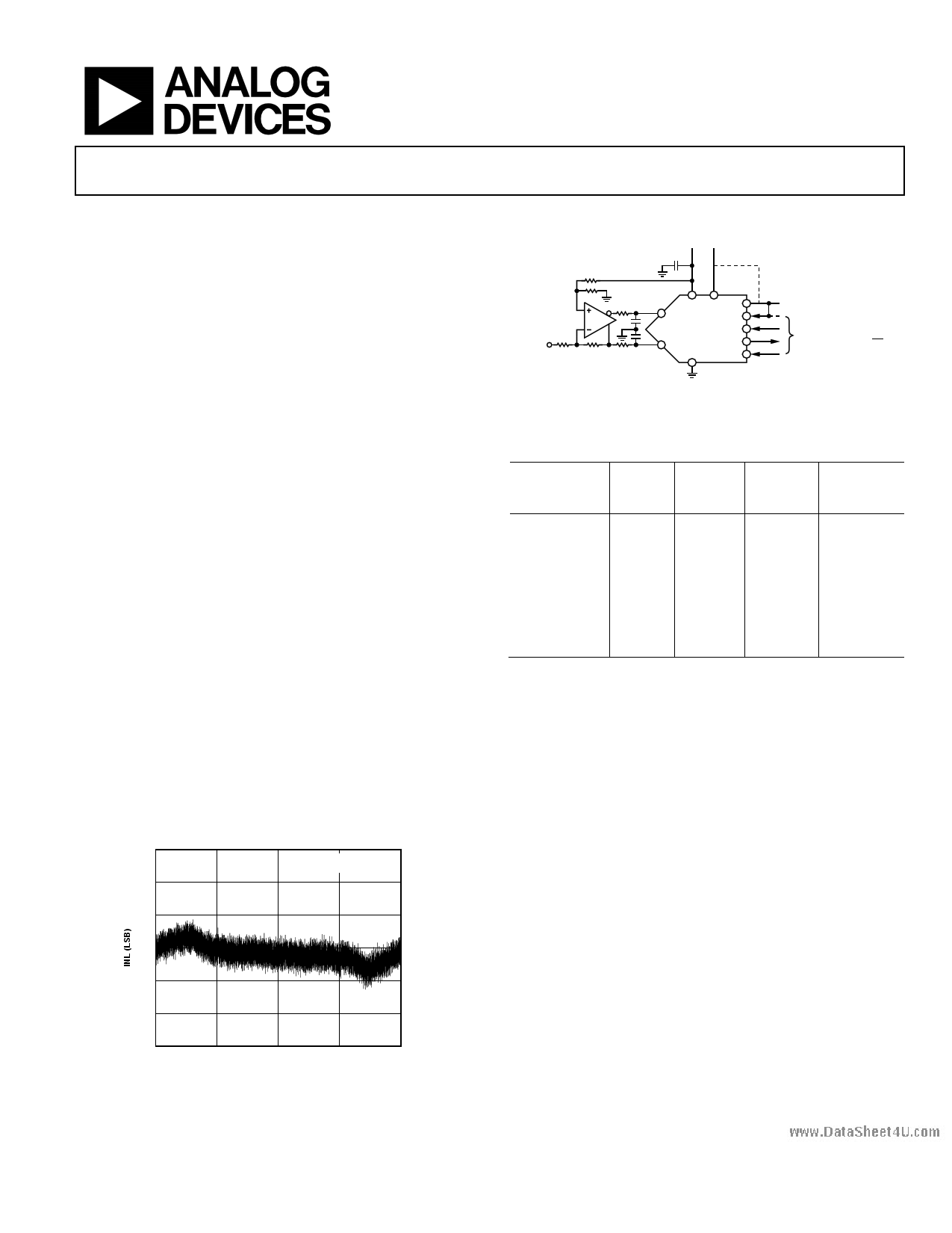
APPLICATION DIAGRAM
+2.3V TO VDD +2.3V TO +5V
±10V, ±5V, ...
ADA4941
REF VDD VIO
IN+ SDI
SCK
IN–
GND
SDO
CNV
+1.8V TO VDD
3- OR 4-WIRE
INTERFACE
(SPI, DAISY CHAIN, CS)
AD7691
Figure 2.
Table 1. MSOP, QFN1 (LFCSP)/SOT-23
14-/16-/18-Bit PulSAR ADC
Type
100
kSPS
250
kSPS
400 kSPS
to
500 kSPS
18-Bit
AD7691 AD7690
16-Bit True
Differential
16-Bit Pseudo
Differential/
Unipolar
14-Bit
AD7684
AD7683
AD7680
AD7940
AD7687
AD7685
AD7694
AD7942
AD7688
AD7693
AD7686
AD7946
ADC
Driver
ADA4941-1
ADA4841-x
ADA4941-1
ADA4841-x
ADA4841-x
ADA4841-x
1 QFN package in development. Contact sales for samples and availability.
GENERAL DESCRIPTION
The AD7691 is an 18-bit, charge redistribution, successive
approximation, analog-to-digital converter (ADC) that operates
from a single power supply, VDD, between 2.3 V and 5 V. It
contains a low power, high speed, 18-bit sampling ADC with no
missing codes, an internal conversion clock, and a versatile
serial interface port. On the CNV rising edge, it samples the
voltage difference between the IN+ and IN− pins. The voltages
on these pins usually swing in opposite phase between 0 V and
REF. The reference voltage, REF, is applied externally and can
be set up to the supply voltage.
Its power scales linearly with throughput.
The SPI-compatible serial interface also features the ability,
using the SDI input, to daisy-chain several ADCs on a single
3-wire bus and provides an optional busy indicator. It is compatible
with 1.8 V, 2.5 V, 3 V, or 5 V logic, using the separate VIO supply.
The AD7691 is housed in a 10-lead MSOP or a 10-lead QFN1
(LFCSP) with operation specified from −40°C to +85°C.
1 QFN package in development. Contact sales for samples and availability.
One Technology Way, P.O. Box 9106, Norwood, MA 02062-9106, U.S.A.
Tel: 781.329.4700
www.analog.com
Fax: 781.461.3113
©2006 Analog Devices, Inc. All rights reserved.
DataSheet4 U .com
1 page 
www.DataSheet4U.com
AD7691
TIMING SPECIFICATIONS
VDD = 4.5 V to 5.25 V, VIO = 2.3 V to VDD, VREF = VDD, all specifications TMIN to TMAX, unless otherwise noted.
Table 4. 1
Parameter
Symbol Min Typ
Conversion Time: CNV Rising Edge to Data Available
Acquisition Time
Time Between Conversions
CNV Pulse Width (CS Mode)
SCK Period (CS Mode)
SCK Period (Chain Mode)
VIO Above 4.5 V
VIO Above 3 V
VIO Above 2.7 V
VIO Above 2.3 V
SCK Low Time
SCK High Time
SCK Falling Edge to Data Remains Valid
SCK Falling Edge to Data Valid Delay
VIO Above 4.5 V
VIO Above 3 V
VIO Above 2.7 V
VIO Above 2.3 V
CNV or SDI Low to SDO D17 MSB Valid (CS Mode)
VIO Above 4.5 V
VIO Above 2.7 V
VIO Above 2.3 V
CNV or SDI High or Last SCK Falling Edge to SDO High Impedance (CS Mode)
SDI Valid Setup Time from CNV Rising Edge (CS Mode)
SDI Valid Hold Time from CNV Rising Edge (CS Mode)
SCK Valid Setup Time from CNV Rising Edge (Chain Mode)
SCK Valid Hold Time from CNV Rising Edge (Chain Mode)
SDI Valid Setup Time from SCK Falling Edge (Chain Mode)
SDI Valid Hold Time from SCK Falling Edge (Chain Mode)
SDI High to SDO High (Chain Mode with Busy Indicator)
VIO Above 4.5 V
VIO Above 2.3 V
tCONV
tACQ
tCYC
tCNVH
tSCK
tSCK
tSCKL
tSCKH
tHSDO
tDSDO
tEN
tDIS
tSSDICNV
tHSDICNV
tSSCKCNV
tHSCKCNV
tSSDISCK
tHSDISCK
tDSDOSDI
0.5
1.8
4
10
15
17
18
19
20
7
7
4
15
0
5
10
3
4
Max
2.2
14
15
16
17
15
18
22
25
15
26
1 See Figure 3 and Figure 4 for load conditions.
Unit
μs
μs
μs
ns
ns
ns
ns
ns
ns
ns
ns
ns
ns
ns
ns
ns
ns
ns
ns
ns
ns
ns
ns
ns
ns
ns
ns
ns
DataSheet4 U .com
Rev. 0 | Page 5 of 28
5 Page 
www.DataSheet4U.com
104 18
SNR
102
100 SINAD 17
98
96 ENOB
16
94
92
15
90
88
86 14
2.3 2.6 2.9 3.2 3.5 3.8 4.1 4.4 4.7 5.0 5.3
REFERENCE VOLTAGE (V)
Figure 13. SNR, SINAD, and ENOB vs. Reference Voltage
AD7691
–105
–110
–115
–120
THD
–125
–130
–135
2.3
SFDR
2.6 2.9 3.2 3.5 3.8 4.1 4.4 4.7 5.0
REFERENCE VOLTAGE (V)
Figure 16. THD, SFDR vs. Reference Voltage
5.3
105
VREF = 5V
100
VREF = 2.5V
95
90
85
80
–55 –35 –15
5
25 45 65 85
TEMPERATURE (°C)
Figure 14. SNR vs. Temperature
105 125
–90
–100
–110
–120
VREF = 5V
VREF = 2.5V
–130
–55 –35 –15
5
25 45 65 85
TEMPERATURE (°C)
Figure 17. THD vs. Temperature
105 125
105
100
95
90
85
80
75
70
0
DataSheet4 U .com
VREF = 5V, –10dB
VREF = 5V, –1dB
VREF = 2.5V, –1dB
VREF = 2.5V, –10dB
25 50 75 100
FREQUENCY (kHz)
Figure 15. SINAD vs. Frequency
125
–60
–70
–80
–90
–100
–110
–120
–130
0
Rev. 0 | Page 11 of 28
VREF = 2.5V, –1dB
VREF = 5V, –1dB
VREF = 5V, –10dB
VREF = 2.5V, –10dB
25 50 75
FREQUENCY (kHz)
Figure 18. THD vs. Frequency
100
125
11 Page | ||
| Páginas | Total 28 Páginas | |
| PDF Descargar | [ Datasheet AD7691.PDF ] | |
Hoja de datos destacado
| Número de pieza | Descripción | Fabricantes |
| AD7690 | Differential ADC | Analog Devices |
| AD7691 | 250 kSPS PulSAR Differential ADC in MSOP/QFN | Analog Devices |
| AD7693 | 500 kSPS PulSAR Differential ADC in MSOP/QFN | Analog Devices |
| AD7694 | 250 kSPS PulSAR ADC in MSOP | Analog Devices |
| Número de pieza | Descripción | Fabricantes |
| SLA6805M | High Voltage 3 phase Motor Driver IC. |
Sanken |
| SDC1742 | 12- and 14-Bit Hybrid Synchro / Resolver-to-Digital Converters. |
Analog Devices |
|
DataSheet.es es una pagina web que funciona como un repositorio de manuales o hoja de datos de muchos de los productos más populares, |
| DataSheet.es | 2020 | Privacy Policy | Contacto | Buscar |